Deposition apparatuses configured for utilizing phased microwave radiation

a phased microwave radiation and apparatus technology, applied in the direction of plasma technique, crystal growth process, chemically reactive gas, etc., can solve the problem that activated species can become deactivated

Inactive Publication Date: 2005-01-25
MICRON TECH INC
View PDF17 Cites 60 Cited by
  • Summary
  • Abstract
  • Description
  • Claims
  • Application Information

AI Technical Summary

Problems solved by technology

However, a problem with remote generation is that an activated species can become deactivated and / or recombined in route from the apparatus in which it is generated to a reaction chamber.

Method used


Image

  • Deposition apparatuses configured for utilizing phased microwave radiation
  • Deposition apparatuses configured for utilizing phased microwave radiation
  • Deposition apparatuses configured for utilizing phased microwave radiation

Examples


Embodiment Construction

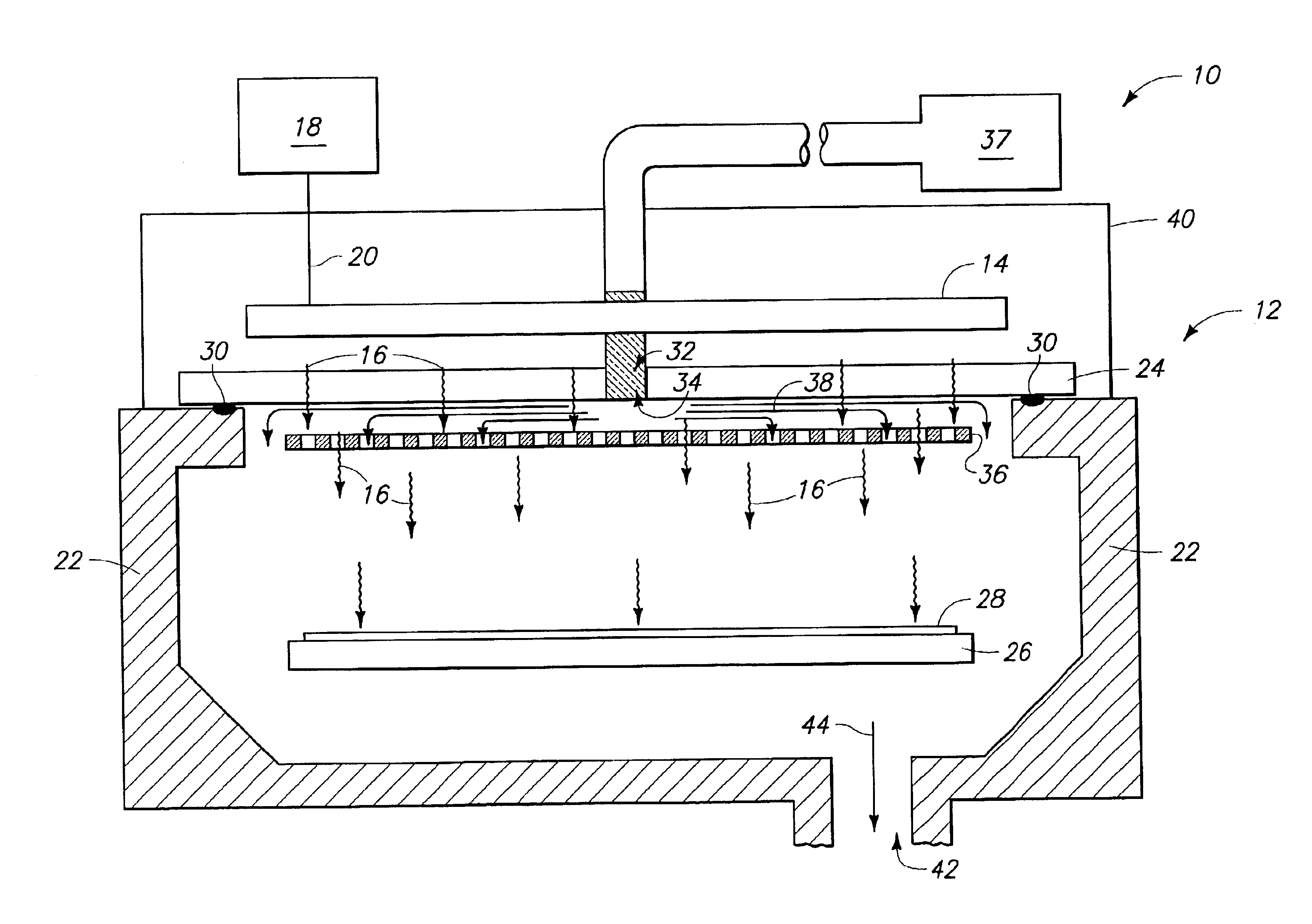
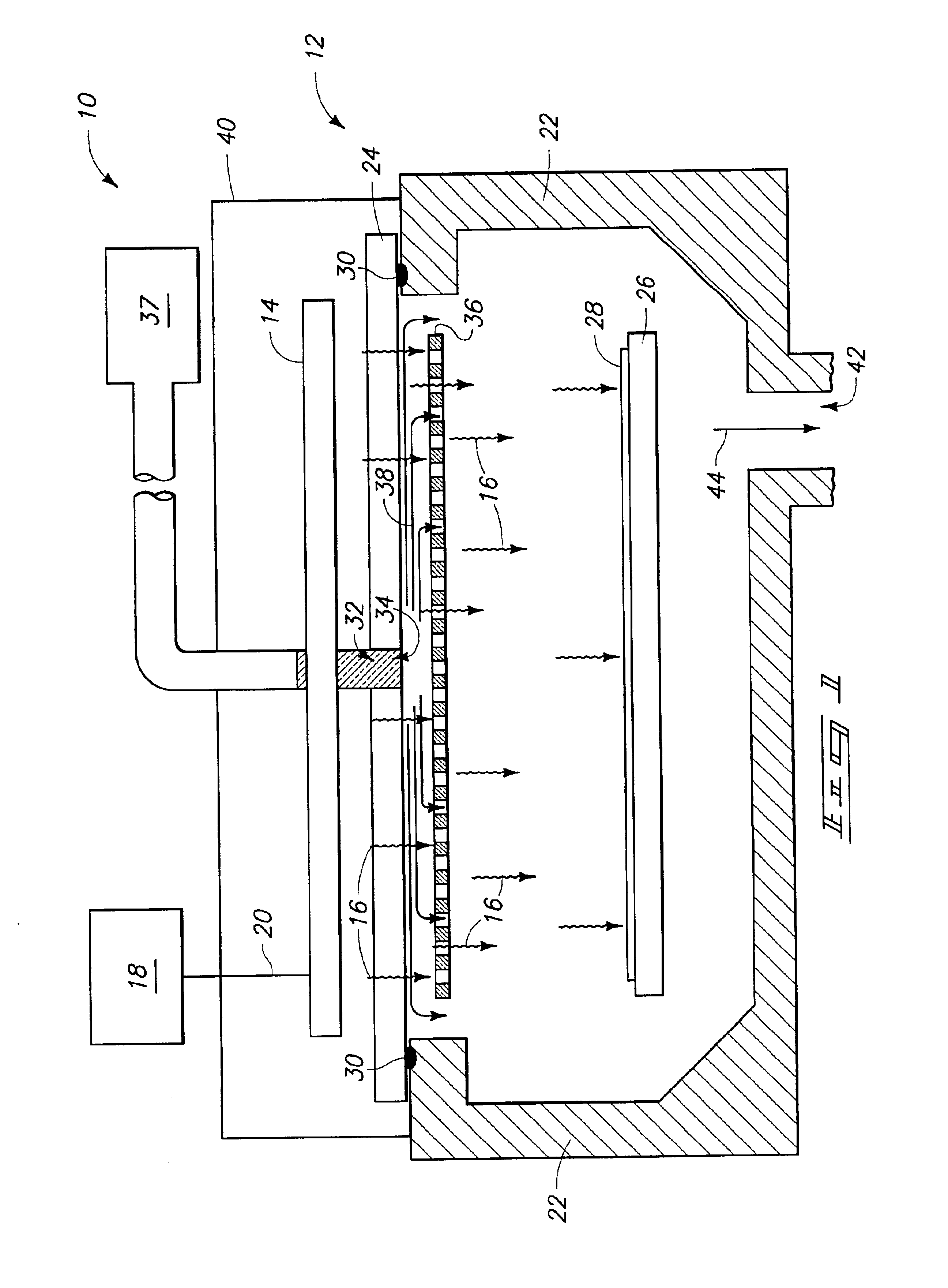
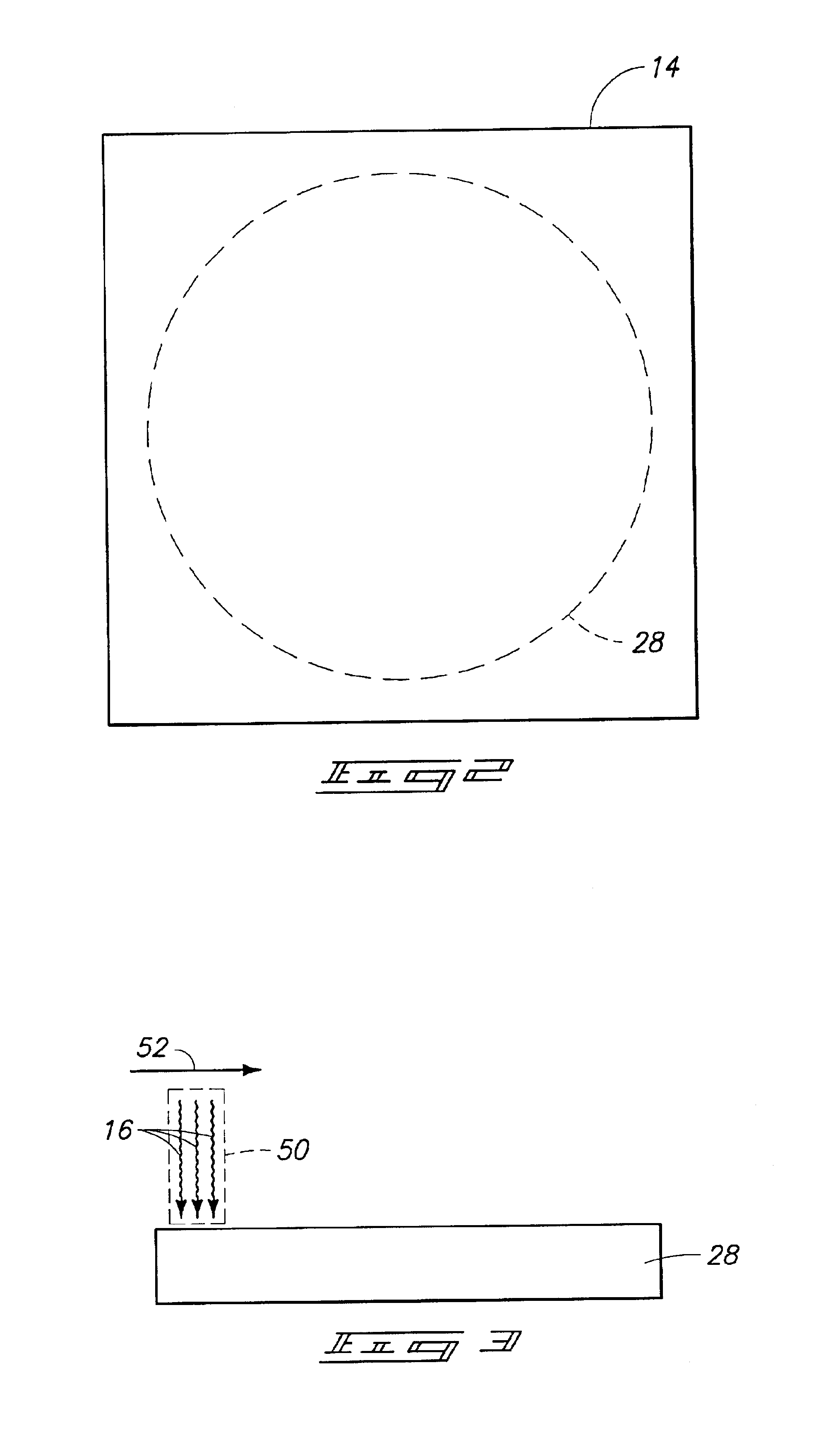
In particular aspects, the present application pertains to atomic layer deposition (ALD) technology. ALD technology typically involves formation of successive atomic layers on a substrate. Such layers may comprise, for example, an epitaxial, polycrystalline, and / or amorphous material. ALD may also be referred to as atomic layer epitaxy, atomic layer processing, etc.

The deposition methods herein are described in the context of formation of materials on one or more semiconductor substrates. In the context of this document, the term “semiconductor substrate” or “semiconductive substrate” is defined to mean any construction comprising semiconductive material, including, but not limited to, bulk semiconductive materials such as a semiconductive wafer (either alone or in assemblies comprising other materials thereon), and semiconductive material layers (either alone or in assemblies comprising other materials). The term “substrate” refers to any supporting structure, including, but not li...


PUM

PropertyMeasurementUnit
wavelengthaaaaaaaaaa
microwave radiationaaaaaaaaaa
temperatureaaaaaaaaaa

Abstract

The invention includes a deposition apparatus having a reaction chamber, and a microwave source external to the chamber. The microwave source is configured to direct microwave radiation toward the chamber. The chamber includes a window through which microwave radiation from the microwave source can pass into the chamber. The invention also includes deposition methods (such as CVD or ALD methods) in which microwave radiation is utilized to activate at least one component within a reaction chamber during deposition of a material over a substrate within the reaction chamber.

Description

TECHNICAL FIELDThe invention pertains to deposition methods utilizing microwave excitation, and in particular applications pertains to chemical vapor deposition (CVD) methods and atomic layer deposition (ALD) methods. The invention also pertains to apparatuses which can be utilized for deposition methods.BACKGROUND OF THE INVENTIONSemiconductor processing in the fabrication of integrated circuitry involves the deposition of layers on semiconductor substrates. Exemplary processes include chemical vapor deposition (CVD) and atomic layer deposition (CVD). CVD and ALD can be conducted within chambers or reactors which retain a single substrate upon a wafer holder or susceptor. One or more precursor gasses are typically provided to a shower head within the chamber which is intended to uniformly provide the reactant gasses substantially homogeneously over the outer surface of the wafer. The precursors react or otherwise manifest in a deposition of a suitable layer atop the substrate. Plas...

Claims


Application Information

Patent Timeline
Patent Type & Authority Patents(United States)
IPC IPC(8): C30B25/10C23C16/511C23C16/50H01J37/32H01Q21/00C23C16/44C23C16/455H01L21/205
CPCC23C16/45525C23C16/45536H01Q21/0087C30B25/105H01J37/32192C23C16/511C23C16/40H01Q21/00C23C16/455
Inventor CARPENTER, CRAIG M.DANDO, ROSS S.CAMPBELL, PHILIP H.
Owner MICRON TECH INC
Why Eureka
Try Eureka