

Method for preparing high-specific surface area graphene material by utilizing strong base chemical treatment
A high specific surface area, chemical treatment technology, applied in the field of graphene material production by chemical treatment, can solve the problems of restricting the application of graphene materials, low theoretical specific surface area of graphene, etc., and achieve high conductivity and increase the specific surface area.
- Summary
- Abstract
- Description
- Claims
- Application Information
AI Technical Summary
Problems solved by technology
Method used
Image


Examples
Embodiment 1
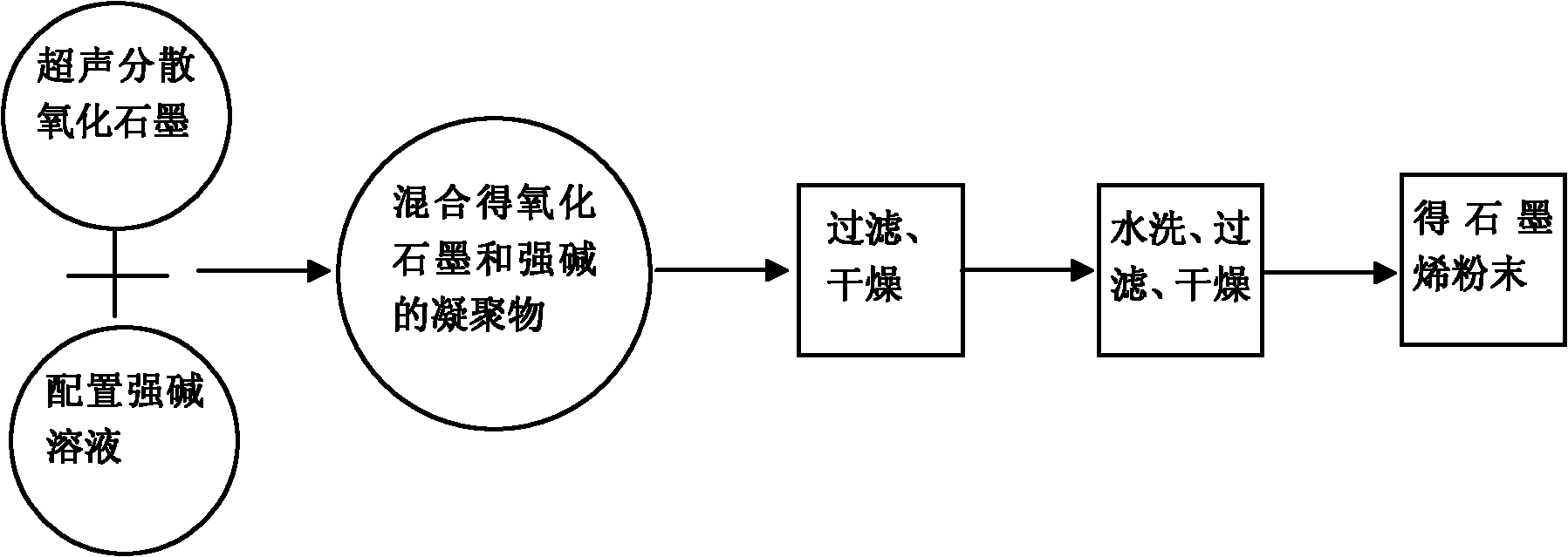
[0020] Utilize the method for potassium hydroxide modified graphene material, comprise following preparation steps:
[0021] 1. Weigh 11.2g of pure potassium hydroxide particles and place them in an alumina beaker, add 20ml of deionized water to obtain a 20mol / L potassium hydroxide aqueous solution;
[0022] 2. Weigh 0.224g of graphite oxide particles and place them in a glass beaker, add 2.24L of deionized water, and use a needle-shaped ultrasonic device to sonicate for 3 hours to obtain a 0.1g / L graphite oxide suspension;
[0023] 3. Pour the potassium hydroxide solution obtained in step 1 into the graphite oxide suspension obtained in step 2, place on a magnetic stirring plate and stir for 30 minutes at a speed of 1000 rpm;
[0024] 4. Pour the condensate obtained in step 3 into a vacuum filter device, and open the vacuum valve for suction filtration; until no water drips down;
[0025] 5. Put the substance obtained in step 4 into a vacuum oven, pump the vacuum to the limi...
Embodiment 2
[0034] Utilize the method for potassium hydroxide modified graphene material, comprise following preparation steps:
[0035] 1. Weigh 0.112g of pure potassium hydroxide particles and place them in an alumina beaker, add 20ml of deionized water to obtain a 0.2mol / L potassium hydroxide aqueous solution;
[0036] 2. Weigh 0.1g of graphite oxide particles and place them in a glass beaker, add 0.01L of deionized water, and use a needle-shaped ultrasonic device to sonicate for 1 hour to obtain a 10g / L graphite oxide suspension;
[0037] 3. Pour the potassium hydroxide solution obtained in step 1 into the graphite oxide suspension obtained in step 2, place on a magnetic stirring plate and stir for 30 minutes at a speed of 200 rpm;
[0038] 4. Pour the condensate obtained in step 3 into a vacuum filter device, and open the vacuum valve for suction filtration; until no water drips down;
[0039] 5. Put the substance obtained in step 4 into a vacuum oven, pump the vacuum to the limit, ...
Embodiment 3
[0048] Utilize the method for sodium hydroxide modified graphene material, comprise following preparation steps:
[0049]1. Weigh 5.6g of pure sodium hydroxide particles and place them in an alumina beaker, add 20ml of deionized water to obtain a 10mol / L potassium hydroxide aqueous solution;
[0050] 2. Weigh 1g of graphite oxide particles and place them in a glass beaker, add 0.2L of deionized water, and use a needle-shaped ultrasonic device to sonicate for 3 hours to obtain a 5g / L graphite oxide suspension;
[0051] 3. Pour the sodium hydroxide solution obtained in step 1 into the graphite oxide suspension obtained in step 2, place on a magnetic stirring plate and stir for 30 minutes at a speed of 1000 rpm;
[0052] 4. Pour the condensate obtained in step 3 into a vacuum filter device, and open the vacuum valve for suction filtration; until no water drips down;
[0053] 5. Put the substance obtained in step 4 into a vacuum oven, pump the vacuum to the limit, set the tempera...
PUM
| Property | Measurement | Unit |
|---|---|---|
| thickness | aaaaa | aaaaa |
| specific surface area | aaaaa | aaaaa |
Abstract
Description
Claims
Application Information