Electron source, image display device manufacturing apparatus and method, and substrate processing apparatus and method

a technology of image display device and manufacturing apparatus, applied in the direction of electrode system manufacture, electrode system manufacturing, electrode system manufacturing, etc., can solve the problem of long time-consuming method

Inactive Publication Date: 2005-01-25
CANON KK
View PDF43 Cites 25 Cited by
  • Summary
  • Abstract
  • Description
  • Claims
  • Application Information

AI Technical Summary

Benefits of technology

[0020]The first manufacturing method, however, requires a larger vacuum chamber and a high-vacuum compatible exhaust device as the electron source substrate becomes larger. The second manufac

Problems solved by technology

The second manufacturing method requires a long time in uniformly introducing gas into a narrow space ins

Method used


Image

  • Electron source, image display device manufacturing apparatus and method, and substrate processing apparatus and method
  • Electron source, image display device manufacturing apparatus and method, and substrate processing apparatus and method
  • Electron source, image display device manufacturing apparatus and method, and substrate processing apparatus and method

Examples


example 1

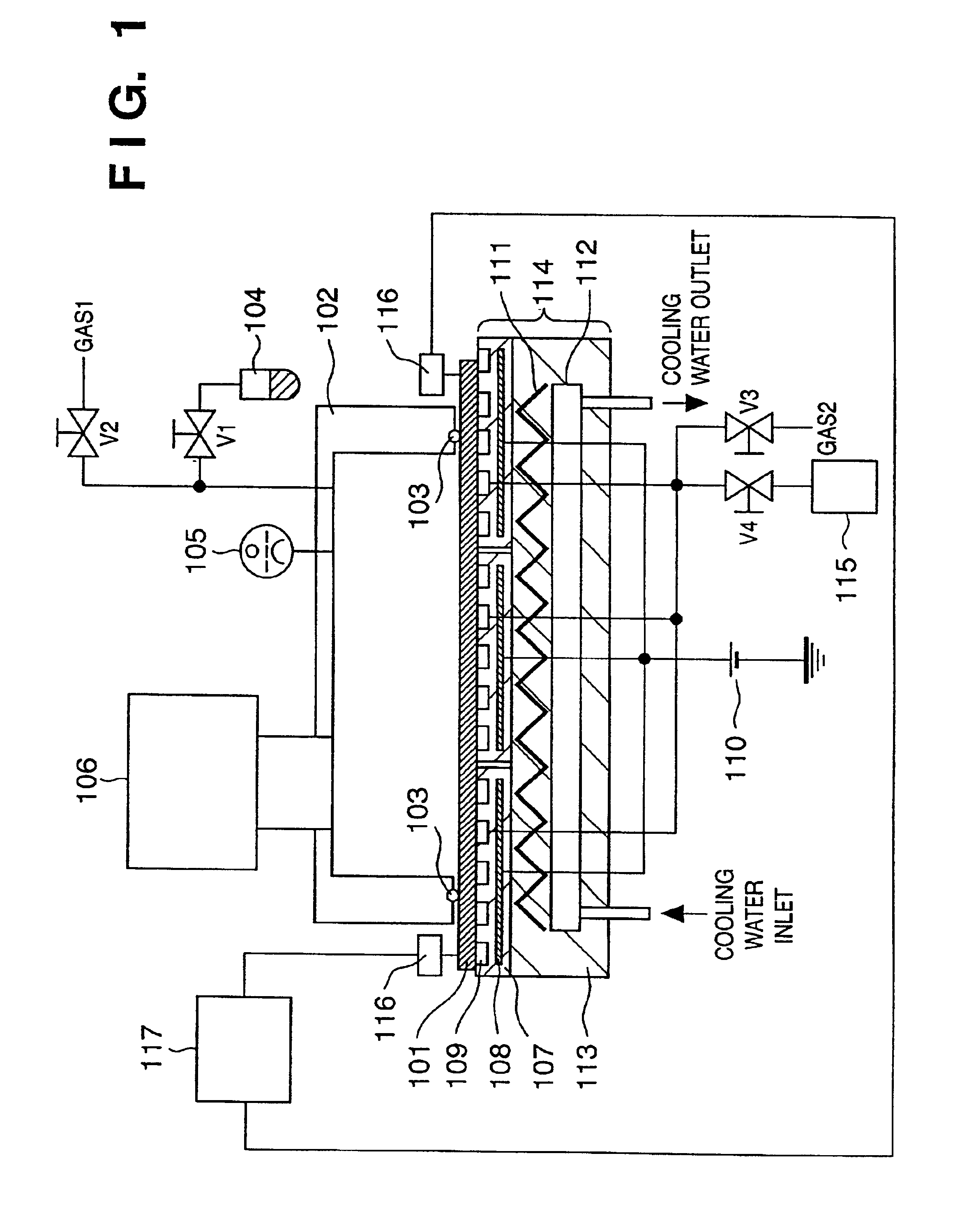
[0117]In Example 1, pairs of electrodes for a surface-conduction type electron-emitting device were arrayed on a substrate in order to fabricate an electron source in which many surface-conduction type electron-emitting devices were arrayed on the substrate. A method of performing etching using the processing apparatus shown in FIG. 4 in patterning the device electrodes will be explained.

[0118]A soda-lime glass substrate having a size of 850 mm×530 mm×2.8 mm (thickness) was used as a substrate 401. An 80-nm thick ITO film was formed on the entire lower surface (second surface) of the substrate 401 by electron beam deposition. This film was for an electrostatic chucking electrode. Surface-conduction type electron-emitting devices and wires shown in FIGS. 6, 7A, and 7B were finally formed on the surface (first surface) of the substrate 401. FIGS. 7A and 7B are showing the structure of a surface-conduction type electron-emitting device 600. In FIGS. 6, 7A, and 7B, reference numeral 600...

example 2

[0128]In Example 2, pairs of electrodes for a surface-conduction type electron-emitting device were arrayed on a substrate in order to fabricate an electron source in which many surface-conduction type electron-emitting devices were arrayed on the substrate. The structure of the electron source is the same as in Example 1, and a description thereof will be omitted.

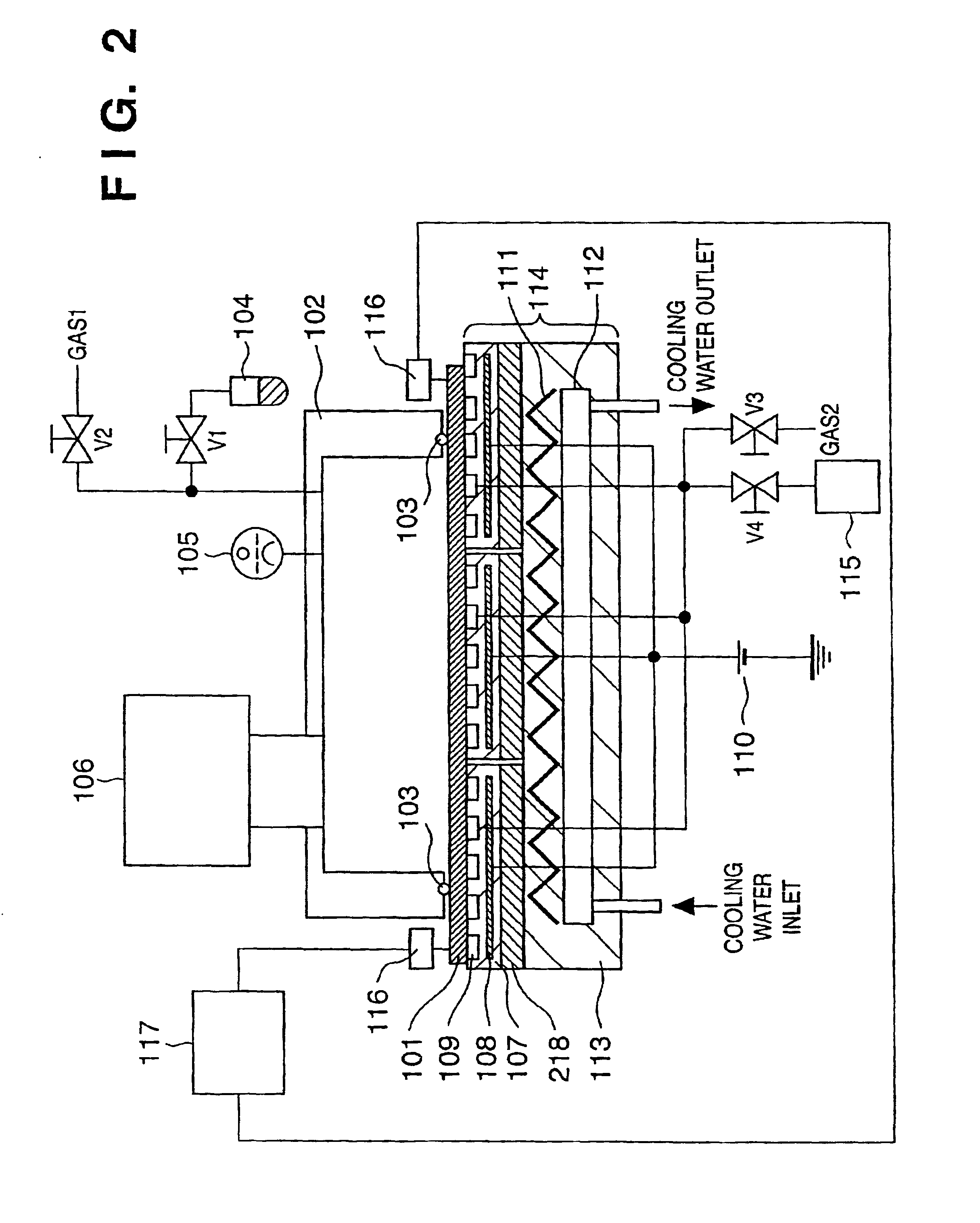
[0129]In Example 2, a method of performing ashing using the processing apparatus shown in FIG. 5 in patterning the device electrodes will be described.

[0130]As electrostatic chucks 107, the processing apparatus shown in FIG. 5 employed six alumina electrostatic chucks 107 in which silver-printed electrodes were buried as electrodes 108 with a size of 200 mm×300 mm×10 mm (thickness). The electrostatic chucks 107 were mounted on independent position adjusting mechanisms 518 using a plurality of screws as a main mechanism, and the position adjusting mechanisms 518 were fixed to a single temperature control means 513. The temp...

example 3

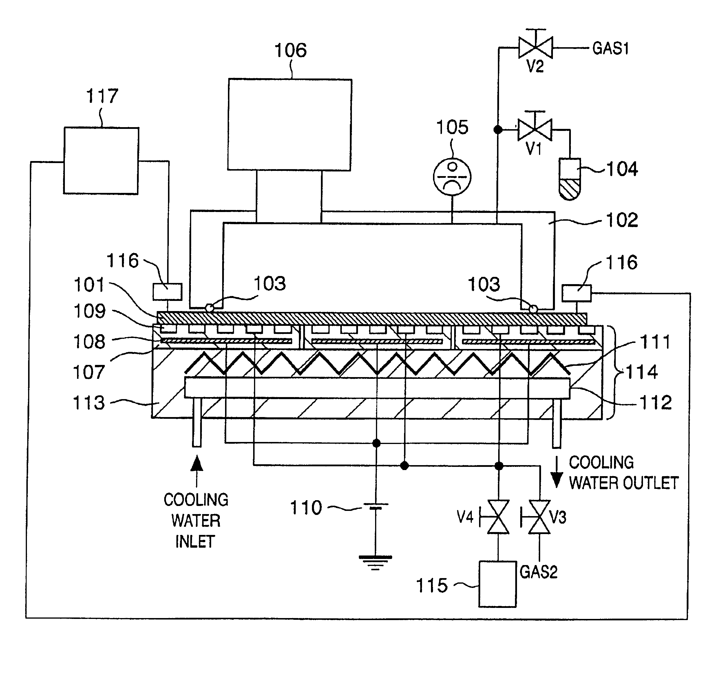
[0136]In Example 3, an electron source in which many surface-conduction type electron-emitting devices were arrayed on a substrate, and an image display device were fabricated using the manufacturing apparatus shown in FIG. 1. The structure of the electron source is the same as in Example 1, and a description thereof will be omitted.

[0137]As lower wires 601, 2,230 wires were formed by printing and baking (baking temperature: 550° C.) Ag paste ink by screen printing on a substrate 101 having pairs of device electrodes 705 and 706 formed by the method of Example 2. As insulating films 603, insulating-glass paste was printed and baked (baking temperature: 550° C.) on parts of the lower wire 601. As upper wires 602, 480 wires were formed by printing and baking (baking temperature: 550° C.) Ag paste ink. Note that the ends of the lower and upper wires 601 and 602 were formed up to 3 mm apart from the edge of the substrate 101 so as to connect the ends to a connection means (terminal) 116...


PUM


Abstract

An electron source/image display device manufacturing apparatus according to this invention includes (A) a support which supports a substrate having a first major surface and a second major surface on which a conductor is arranged, and includes a plurality of electrostatic chucks each having a conductive member, (B) a vessel which has a gas inlet port and an exhaust port, and covers part of the first major surface, (C) a valve connected to the inlet port to introduce gas into the vessel, (D) an exhaust system connected to the exhaust port to exhaust the gas from the vessel, and (E) a power supply for applying a predetermined potential difference between the conductor and the conductive member. This apparatus arrangement enables easy, stable processing in the “forming” and “activation” steps.

Description

FIELD OF THE INVENTION[0002]The present invention relates to an electron source, an image display device manufacturing apparatus and method, and a substrate processing apparatus and method for executing steps of forming a film on a substrate.BACKGROUND OF THE INVENTION[0003]A plasma display, EL display device, and image display device using an electron beam are known as emissive type image display devices. In recent years, demands are arising for larger-screen, higher-resolution image display devices, and needs for emissive type image display devices are increasing.[0004]For example, as an emissive type image display device using an electron beam, the present applicant has applied a thin image display device in which an electron source for generating an electron beam is arranged in an envelope that is made up of a face plate, rear plate, and outer frame and can maintain vacuum, surface-conduction type electron-emitting devices are arrayed in a matrix as the electron source, an elect...

Claims


Application Information

Patent Timeline
IPC IPC(8): H01J9/02H01J1/30H01L21/302H01L21/3065H01L21/683
CPCH01J9/027H01J2201/3165H01J1/30
Inventor SATO, YASUE
Owner CANON KK
Why Eureka
Try Eureka