Optical transmitter
a technology of optical transmitters and lds, applied in the field of optical transmitters, can solve the problems of reducing costs, limiting the size of the ld, and requiring a lot of time for axis alignment, and achieves the effects of low coupling efficiency between the pd and the ld, easy chip mounting and wire bonding, and increased us
- Summary
- Abstract
- Description
- Claims
- Application Information
AI Technical Summary
Benefits of technology
Problems solved by technology
Method used
Image

Examples
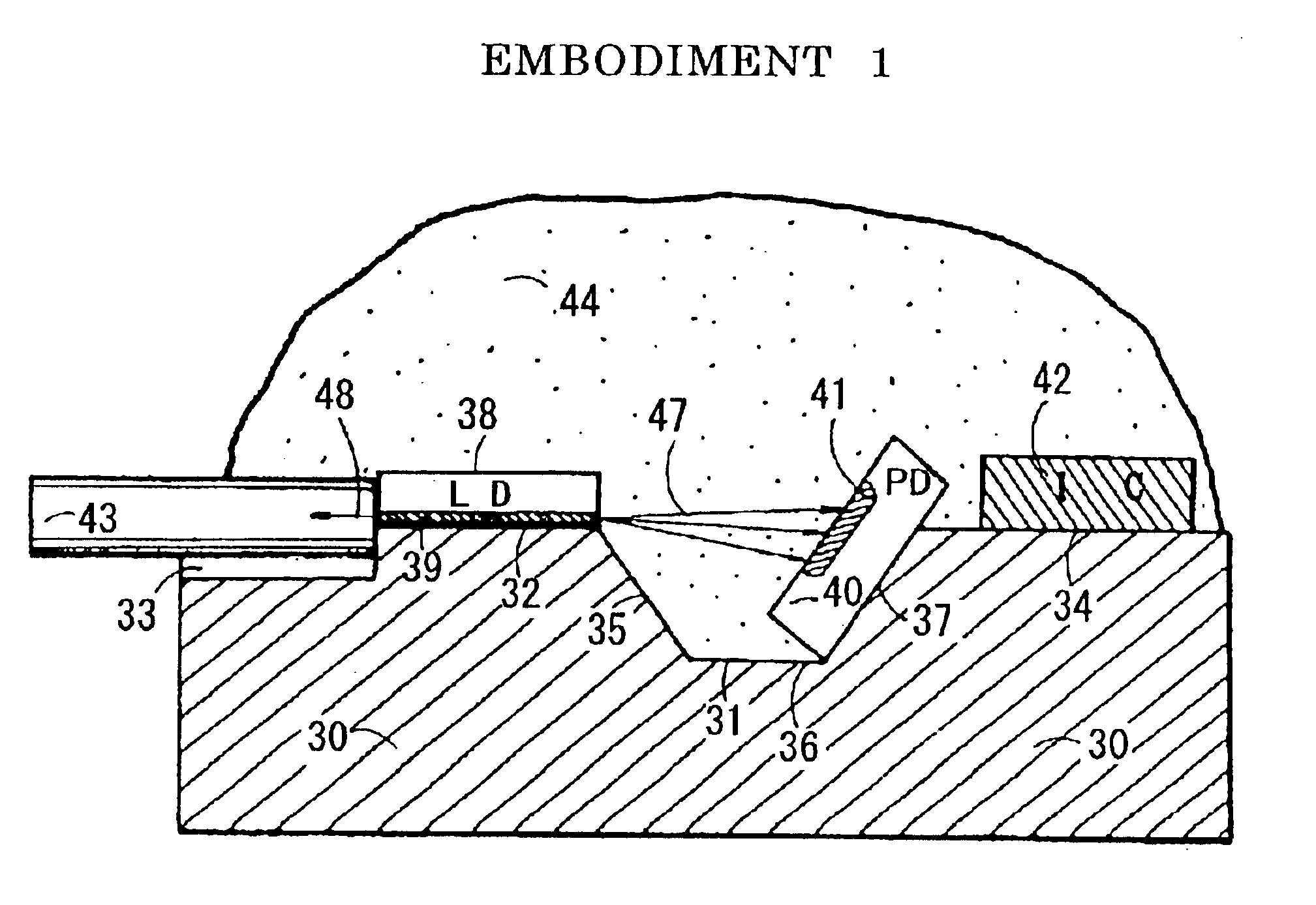
embodiment 1
[Embodiment 1; α=45° (Top-incident PD)(FIGS. 5 and 6)]
A module having a structure of FIG. 5 was manufactured. A substrate used herein is a ceramic substrate of alumina (Al2O3) of 4 mm in length, 3 mm in width, and 1.2 mm in thickness.
First, a fixed groove 33 for an optical fiber, the metallized pattern for fixing a semiconductor LD, and a concave groove 31 for fixing the monitor PD were formed on the substrate. The metallized pattern could be formed by printing, vapor deposition, or sputtering. Since a space at the rear part of the substrate exists, a driver IC can be mounted there. When a driver IC 42 had been mounted, a metallized pattern for the driver IC was provided together therewith. If the driver IC is mounted, the device can be used for the high-bit-rate transmission of 5 Gbps to 10 Gbps because the distance to the LD is extremely short. However, the driver IC can, of course, be omitted. If so, since a driver IC is disposed outside, the driver IC and the LD are connected to...
embodiment 2
[Embodiment 2; α=45° (Rear-incident PD)(FIG. 8)]
A rear-incident PD was used as the monitor PD as shown in FIG. 8. Except for this, a module was manufactured in almost the same way as in Embodiment 1.[Substrate] Ceramic, Alumina (Al2O3)4 mm in length×3 mm in width×1.2 mm in thickness[Semiconductor LD] 1.3 μm InGaAsP-LD0.3 mm×0.3 mm×0.12 mmt [Monitor PD] Rear-incident InGaAs-PDDetecting area 0.2 mm in diameter0.4 mm×0.4 mm×0.12 mmt [Exterior of module] 4 mm in length×3 mm in width×2.5 mm in height
The rear light 47 of the LD 38 striking the rear face of the PD 46, was thereafter refracted, and guided to the detecting area. Since the refractive index of the PD had been high, the amount of light that reached the detecting area was large. A lens did not need to be provided on the rear face of the PD. From the viewpoint of performance, the monitor current advantageously averaged 300 μA, and the relationship between the PD and LD was stable, and an excellent waveform was observed during hig...
PUM
 Abstract
Description
Claims
Application Information
 - R&D
- Intellectual Property
- Life Sciences
- Materials
- Tech Scout
- Unparalleled Data Quality
- Higher Quality Content
- 60% Fewer Hallucinations
Browse by: Latest US Patents, China's latest patents, Technical Efficacy Thesaurus, Application Domain, Technology Topic, Popular Technical Reports.
© 2025 PatSnap. All rights reserved.Legal|Privacy policy|Modern Slavery Act Transparency Statement|Sitemap|About US| Contact US: help@patsnap.com