Semiconductor device and manufacturing the same

a technology of semiconductor devices and semiconductors, applied in semiconductor devices, semiconductor/solid-state device details, electrical equipment, etc., can solve problems such as high cos

Inactive Publication Date: 2005-01-25
RENESAS ELECTRONICS CORP
View PDF2 Cites 14 Cited by
  • Summary
  • Abstract
  • Description
  • Claims
  • Application Information

AI Technical Summary

Benefits of technology

Having made studies about the cost reduction of a high frequency power amplifier for a base station, the present inventor reviewed a sealing structure (package structure) as a main cause of high cost.
It is an object of the present invention to reduce the material cost, reduce the cost of an assembling work including a sealing work, reduce the inspection cost, and thereby reduce the semiconductor device manufacturing cost.

Problems solved by technology

Having made studies about the cost reduction of a high frequency power amplifier for a base station, the present inventor reviewed a sealing structure (package structure) as a main cause of high cost.

Method used


Image

  • Semiconductor device and manufacturing the same
  • Semiconductor device and manufacturing the same
  • Semiconductor device and manufacturing the same

Examples


first embodiment

(First Embodiment)

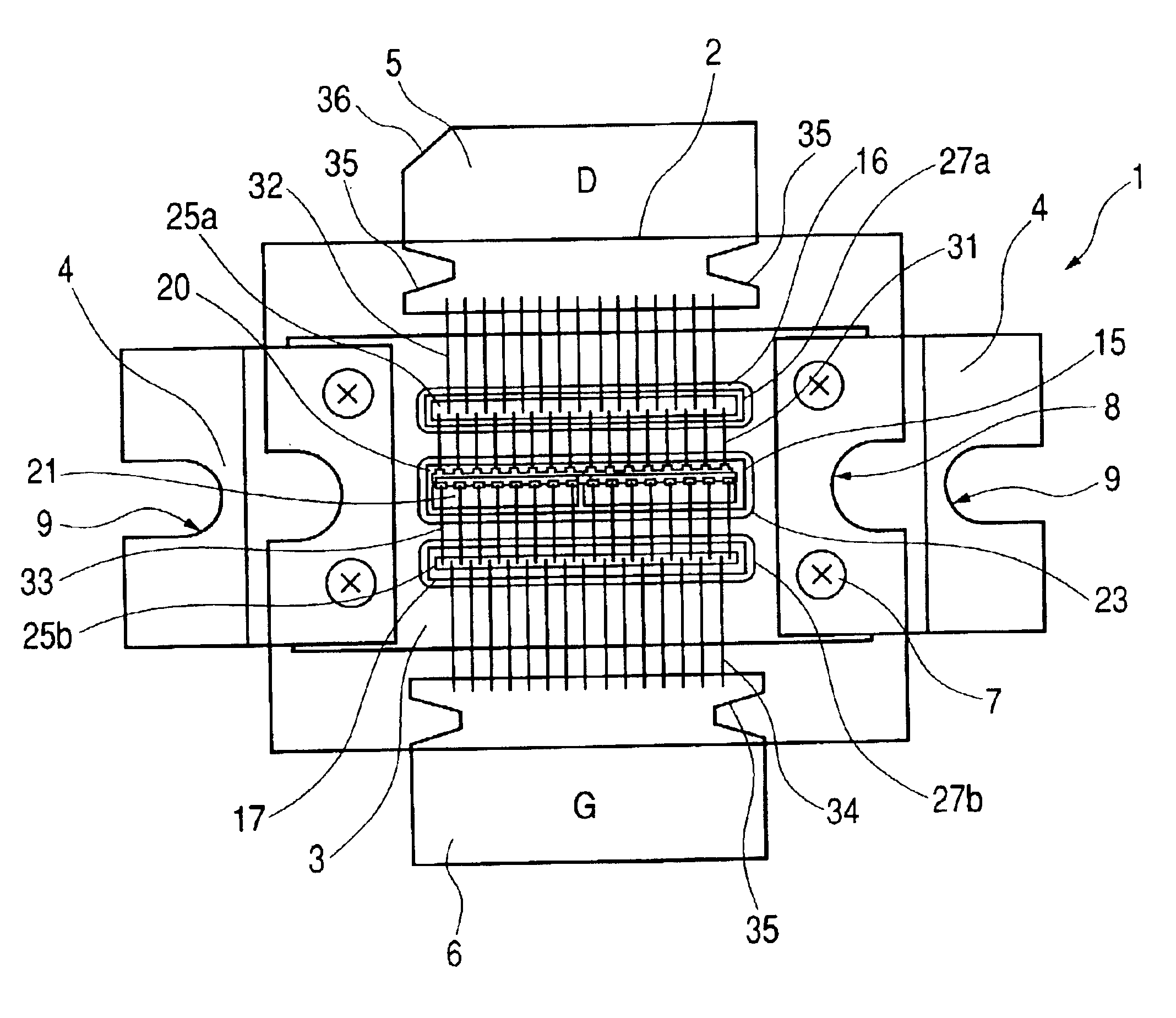
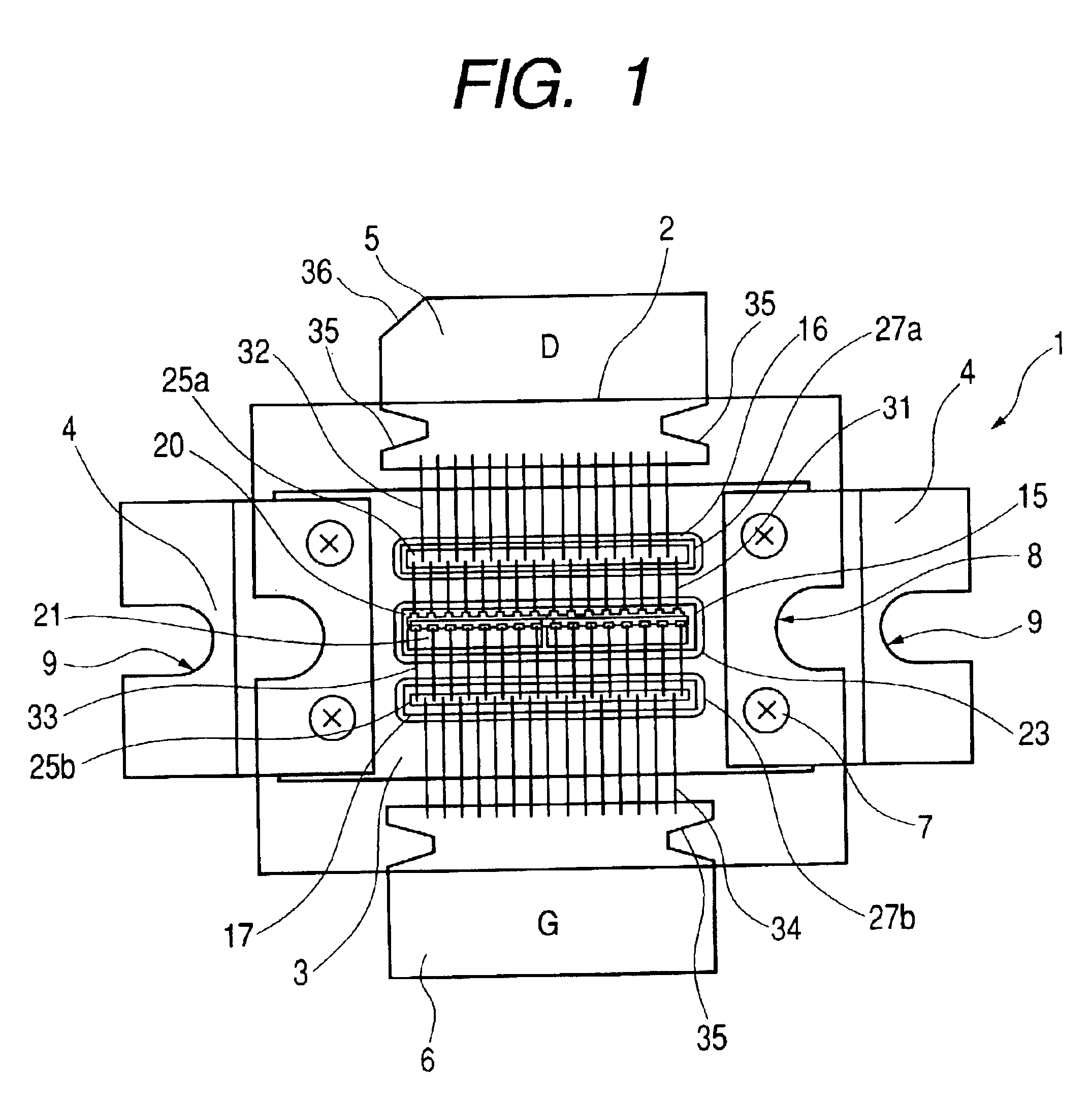
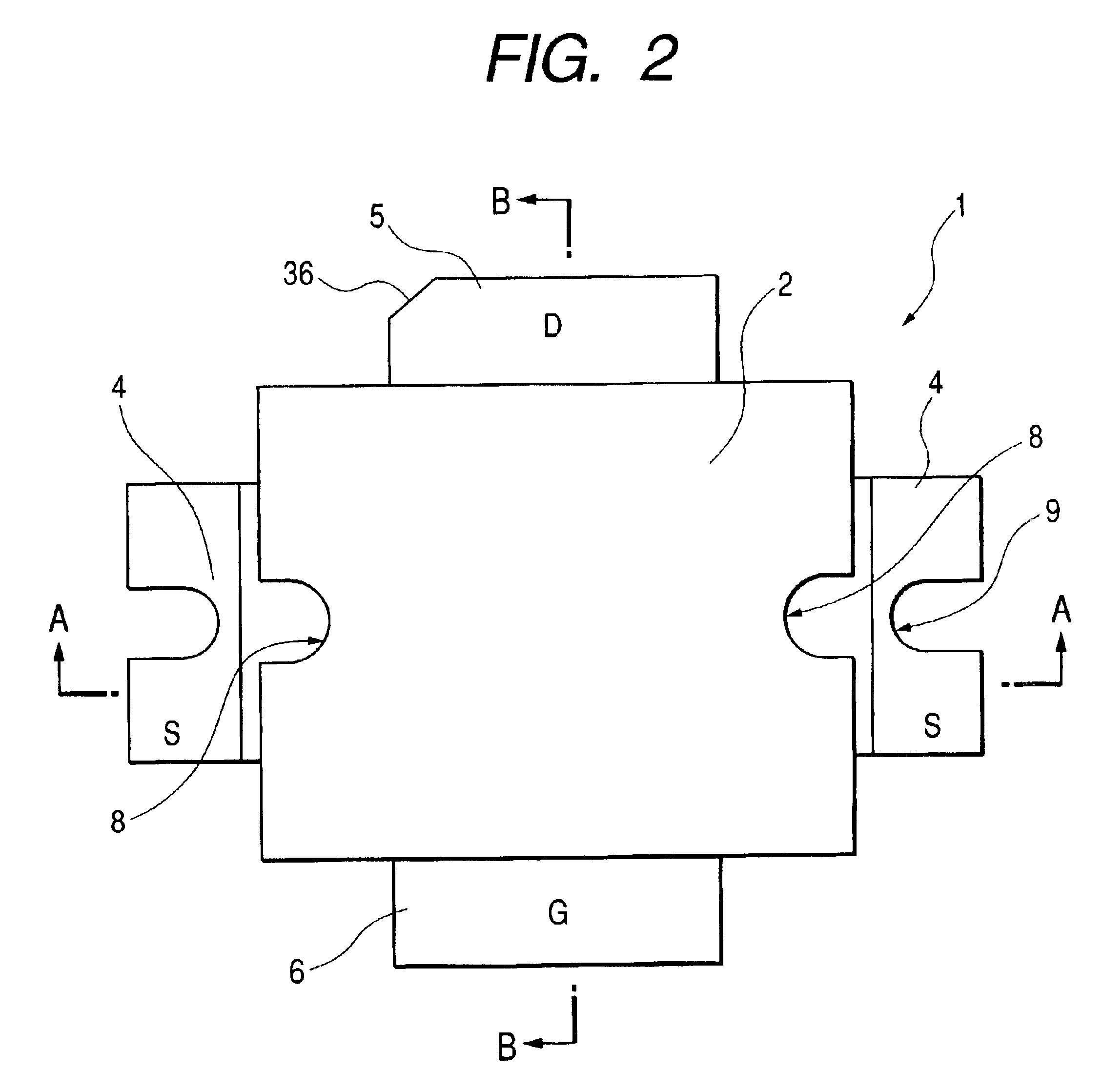
FIGS. 1 to 18 are concerned with a semiconductor device according to an embodiment (first embodiment) of the present invention, of which FIGS. 1 to 7 are concerned with the structure of the semiconductor device and FIGS. 8 to 17 are concerned with the manufacture of the semiconductor device. In this first embodiment, a description will be given below about an example in which the present invention is applied to a high frequency power amplifier (a high frequency power amplifier module) for a base station, as a semiconductor device.

The semiconductor device of this first embodiment, i.e., a high frequency power amplifier module for a base station, indicated at 1, has such a structure as shown in FIGS. 1 to 7, of which FIG. 1 is a perspective plan view, FIG. 2 is a plan view, FIG. 3 is a front view, FIG. 4 is a side view, FIGS. 5 and 6 are schematic sectional views taken along lines A—A and B—B in FIG. 2, and FIG. 7 is a partially enlarged sectional view.

In appearance,...

second embodiment

(Second Embodiment)

FIGS. 19 to 21 illustrate a semiconductor device according to another embodiment (second embodiment) of the present invention, of which FIG. 19 is a perspective plan view showing the structure of the semiconductor device, FIG. 20 is a schematic sectional view of the semiconductor device, and FIG. 21 is a schematic sectional view in another section of the semiconductor device.

According to the semiconductor device of this second embodiment, in the structure of the first embodiment there is adopted a double molded structure in which, as shown in FIGS. 19 to 21, the semiconductor chips 15, 16, 17 and the wires 31 to 34 are covered with undercoat resin 56, and the undercoat resin 56, etc. are sealed with the seal member 2.

The heat resistance of transfer molding resins presently in practical use is 150° C. or so, thus giving rise to the problem that it is impossible to cope with the junction temperature of Tj≧175° C. required of a power FET for a base station. Besides, ...

third embodiment

(Third Embodiment)

FIG. 24 is a plan view of a semiconductor device according to a further embodiment (third embodiment) of the present invention and FIG. 25 is a front view thereof. This third embodiment shows an example in which the drain and gate leads 5, 6 of the structures described in the first embodiment are each arranged side by side in a plural number. In this third embodiment, two sets of drain and gate leads 5, 6 are arranged side by side. With such a structure, it is possible to increase the output.


PUM

PropertyMeasurementUnit
thicknessaaaaaaaaaa
temperatureaaaaaaaaaa
thicknessaaaaaaaaaa

Abstract

A semiconductor device is designed to resist warpage of a heat sink with an inexpensive construction. The device comprises a heat sink, a pair of screwing pieces having inner end portions connected to ends of the heat sink and outer end portions formed with through spaces for screwing, a semiconductor chip fixed to a main surface of the heat sink, a seal covering a back side of the heat sink and partially covering the paired screwing pieces, first and second leads having outer end portions projecting from the seal member and inner end portions within the seal member near respective side faces of the heat sink, and conductive wires electrically connecting the leads and predetermined electrodes of a semiconductor chip.

Description

BACKGROUND OF THE INVENTIONThe present invention relates to a semiconductor device and a method of manufacturing the same. Particularly, the invention is concerned with a technique which is effectively applicable to a manufacturing technique for a high frequency power amplifier (high frequency power amplifier module) for a base station in a radio communication system such as a cellular communication system.SUMMARY OF THE INVENTIONIn a radio communication system such as a cellular communication system, a portable telephone set (a portable terminal) is connected to a base station adjacent to a telephone network by a speaker's operation of the telephone set, then is connected successively to a single or plural base stations, and finally a portable terminal of the party being called is called (originating a call), thereafter the portable telephone set assumes a state which permits talking with the called party. In this case, the base station amplifies the received signal and transfers t...

Claims


Application Information

Patent Timeline
Patent Type & Authority Patents(United States)
IPC IPC(8): H01L21/02H01L21/60H01L21/56H01L23/28H01L23/31H01L23/02H01L23/40H01L23/04H01L23/12H01L23/36H01L23/29H01L23/08H01L23/48H01L23/34H01L25/07H01L25/18H01L21/44H01L21/48H01L21/50H01L21/607H01L23/433H01L23/495H01L23/66
CPCH01L23/3135H01L23/4006H01L23/4334H01L23/49562H01L23/49568H01L23/49575H01L23/66H01L24/48H01L24/49H01L24/78H01L24/85H01L24/29H01L24/45H01L2223/6644H01L2224/45124H01L2224/48091H01L2224/48137H01L2224/48247H01L2224/48472H01L2224/48699H01L2224/4911H01L2224/49175H01L2224/73265H01L2224/78313H01L2224/85181H01L2924/01002H01L2924/01004H01L2924/01005H01L2924/01006H01L2924/01013H01L2924/01014H01L2924/01015H01L2924/01028H01L2924/01047H01L2924/01074H01L2924/01078H01L2924/01079H01L2924/01082H01L2924/01322H01L2924/01327H01L2924/014H01L2924/13091H01L2924/16195H01L2924/19041H01L2924/19042H01L2924/30105H01L2924/30107H01L2924/3011H01L2924/3511H01L2924/0132H01L2224/83805H01L2924/01023H01L2924/01033H01L2224/29111H01L2924/15747H01L2924/15763H01L2224/32245H01L2224/29144H01L2224/85099H01L2924/1306Y10T29/49121H01L2924/00014H01L2924/00H01L2924/01026H01L2924/0105H01L2924/3512H01L2924/01042H01L2924/30111H01L2924/181H01L2224/85205H01L2924/00011H01L2924/12036H01L2224/83205H01L2924/00012H01L2224/85399H01L2224/05599
Inventor ITO, MAMORU
Owner RENESAS ELECTRONICS CORP
Why Eureka
Try Eureka