Control circuit for charging and discharging, illuminating apparatus and driving method thereof

a control circuit and illuminating technology, applied in static indicating devices, instruments, electrochemical generators, etc., can solve the problems of residual charge, undesirable current, residual charge, etc., and achieve high display quality, high-quality display, and substantial elimination of the influence of residual charg

Inactive Publication Date: 2005-01-25
NICHIA CORP
View PDF8 Cites 11 Cited by
  • Summary
  • Abstract
  • Description
  • Claims
  • Application Information

AI Technical Summary

Benefits of technology

In such a construction, an undesirable charge remaining in each light-emitting element or in its periphery is charged in the charging element during driving-off status, and is discharged during driving-on status. An influence caused by a residual charge can be substantially eliminated in driving-on status, in which the desired light-emitting elements emit, and it is possible to provide an illuminating apparatus with high display quality.
In the present invention, a discharging path refers to a path to release a charge from a charging element. A discharging path is connected so that the whole of or a part of accumulated charge flows from a charging element to a ground or a desired discharging point. It is not always necessary to normally connect. A discharging path can include a switching circuit or a rectifier such as a transistor for controlling a discharging timing. A charge can be discharged to a ground. In addition, A charge can be discharged so as to act as the whole of or a part of current for a driven element. This does not waste a residual charge and can make effective use of it by reusing. Therefore, it is possible to save power and to obtain an eco-friendly and energy-recyclable circuit.

Problems solved by technology

However, there is a problem that electric charge remains in light-emitting diodes (light-emitting elements) connected to the common source line, which is not selected, or light-off status, while the light-emitting diodes (light-emitting elements), which are connected to the selected common source line, emit.
Such a residual charge, which remains in the unselected period, produces an undesirable current when the common source line is selected.
Such produced undesirable current reduces display quality because of undesirable-emission that the light-emitting diode, which is controlled not emitting, slightly emits, and insufficient contrast in display image.
Therefore, the circuit cannot prevent the undesirable-emission that the light-emitting diode, which is controlled not emitting, slightly emits.
For example, there is the same problem in voltage control elements in a liquid crystal display.
Especially, in a large-scale display with long traces or numbers of traces, there is a problem such as an undesirable emission, false displaying, and false driving.

Method used


Image

  • Control circuit for charging and discharging, illuminating apparatus and driving method thereof
  • Control circuit for charging and discharging, illuminating apparatus and driving method thereof
  • Control circuit for charging and discharging, illuminating apparatus and driving method thereof

Examples


embodiment 1

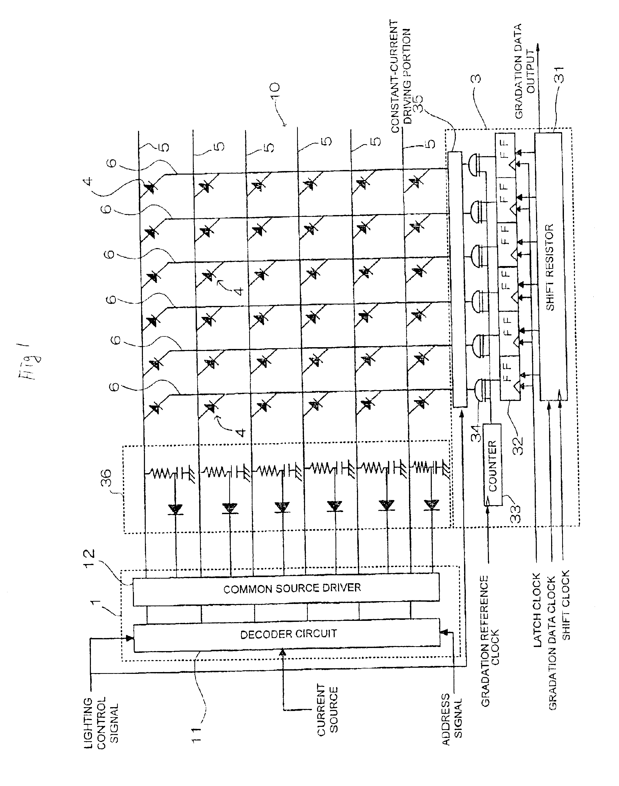
FIG. 1 is a block diagram schematically showing a construction of an LED display apparatus according to an embodiment of the present invention. The undesirable-emission-preventing circuit 36 in the invention is provided for each common source line. The LED display apparatus of this embodiment comprises an LED display portion including a plurality of light-emitting diodes 4 arranged in a matrix with m rows and n columns, a current line provided for each column and connected to a cathode terminal of each of the light-emitting diodes 4 arranged in each column, and a common source line provided for each row and connected to an anode terminal of each of the light-emitting diodes 4 arranged in each row; a current-source switching circuit 1, which has m of switching circuits connected to the corresponding common source lines 5, capable of connecting the common source line addressed by an address signal input to a current source in the light-on period determined by the lighting control sign...

embodiment 2

The following description will describe the second embodiment according to the present invention with reference to the drawings. FIG. 7 to FIG. 10 show a second driving method according to the present invention. The second driving method is an embodiment, in which a residual charge in a current line is eliminated when scanning changes into the next common switch line.

In FIG. 7 to FIG. 10, current lines (driving lines), common switch lines (scanning lines), charge elements connected at locations corresponding to intersections of them, a common switch line scanning circuit, a current line driving circuit, an anode control circuit for charging and discharging, and a driving control circuit are shown as A1-A256, B1-B64, E1,1-E256,64, 41, 42, 43, and 44 respectively.

The common switch line scanning circuit 41 has scanning switches 451-4564 for sequentially scanning common switch lines B1-B64. One terminal of each of the scanning switches 451-4564 is connected to a reverse bias Vcc (10 V, ...

embodiment 3

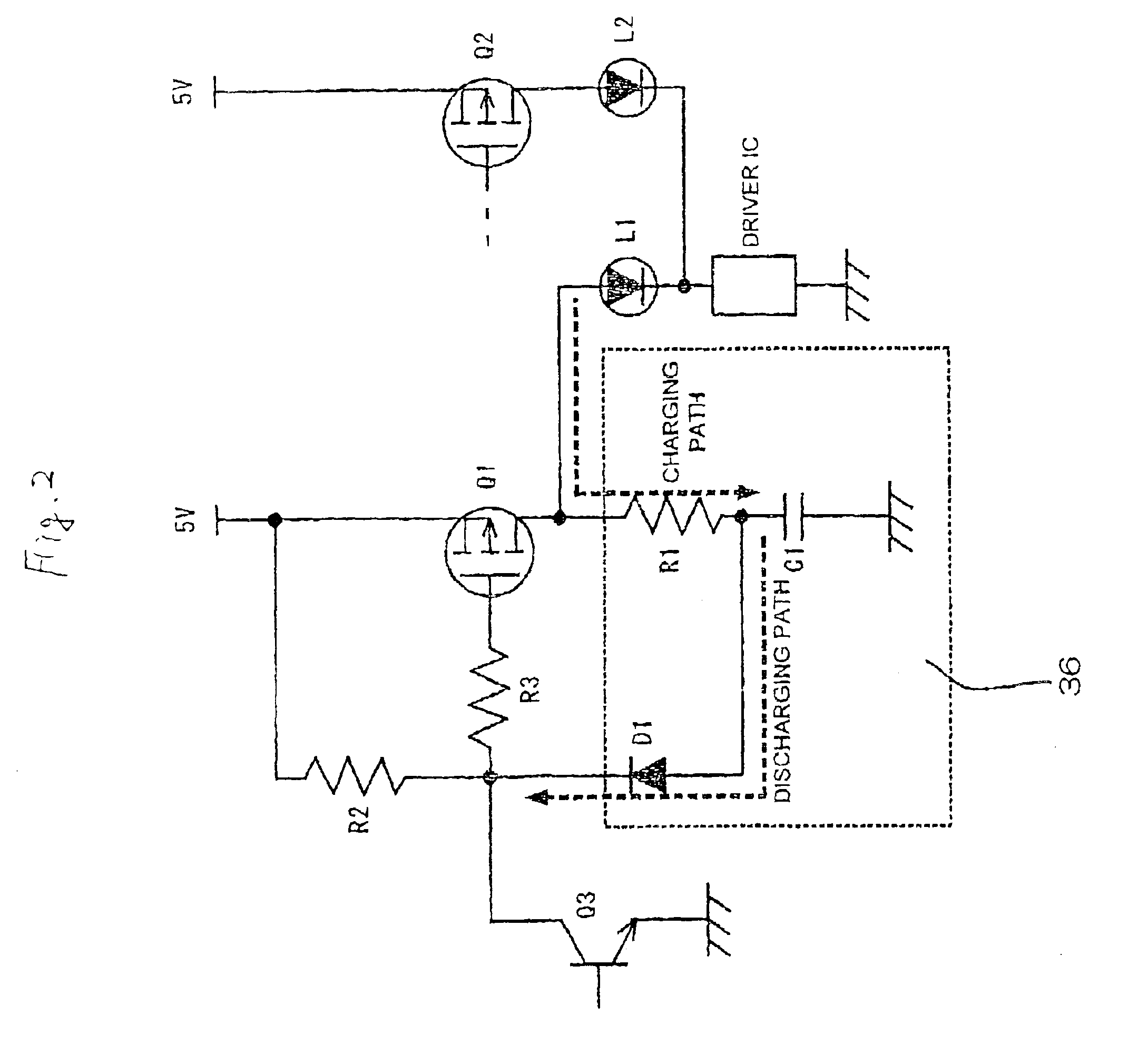
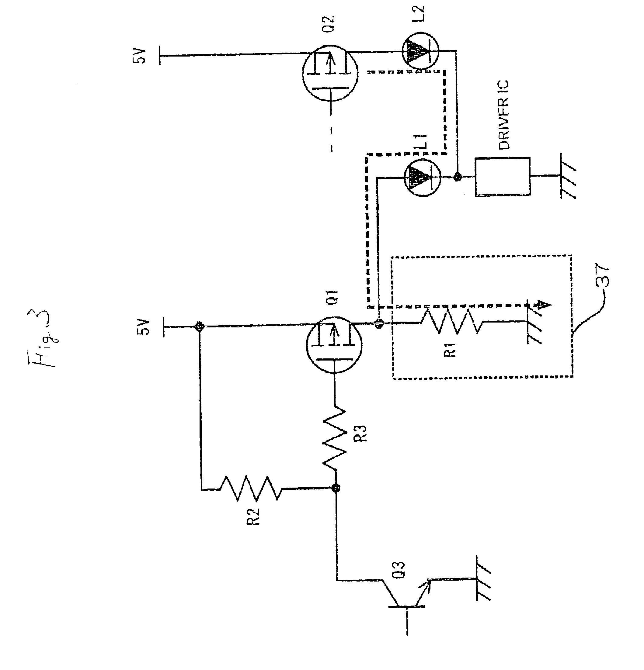
The following description will describe an undesirable-emission-preventing circuit of a control circuit for charging and discharging of the embodiment 3 according to the present invention with reference to FIG. 12.

In FIG. 12, a switch (SW2) operates in synchronization with a switch (SW1). When the switch (SW1) is connected to a power supply (5V), the switch (SW2) is opened, and when the switch (SW1) is grounded, the switch (SW2) is grounded. In addition, when the switch (SW1) is grounded, a transistor (Q1) is turned on, and a light-emitting diode (L1) emits corresponding to a driving status of a driver IC. At this time, the switch (SW2) is grounded, and a residual charge accumulated in a capacitor (C1) is discharged through the switch (SW2).

When the switch (SW1) is connected to the power supply (5V), the transistor (Q1) is turned off, and the light emitting diode (L1) is in a driven-off status irrespective of a driving status of the driver IC. While a transistor (Q1) turns off, the ...


PUM

PropertyMeasurementUnit
resistanceaaaaaaaaaa

Abstract

It is an object of the present invention to provide a control circuit for charging and discharging (43) etc., which can prevent an undesirable-emission caused by a residual charge, capable of obtaining a high-quality display and so on. The control circuit for charging and discharging (43) includes a driven element (E1,1-E256,64) with a driving-on status and a driving-off status; a charging element, whose one end is grounded; and a driving circuit (44), which is connected to the driven element (E1,1-E256,64), for controlling the driving-on status or the driving-off status in the driven element. The control circuit further includes a charging path, which is connected to the driven element (E1,1-E256,64), for charging the charging element with a residual charge, which is produced in the driven element (E1,1-E256,64) and / or a line connected to the driven element (E1,1-E256,64) during the driving-on status, and a discharging path, which is connected to the charging path, for discharging the residual charge from the charging element to a ground in the driving-on status.

Description

This application is based on Application No. 2002-142432 filed in Japan on May 17, 2002, and No. 2003-107044 filed in Japan on Apr. 10, 2003, the contents of which are incorporated hereinto by references.BACKGROUND OF THE INVENTION1. Field of the InventionThe present invention relates to a control circuit for charging and discharging, an illuminating apparatus and a driving method thereof, which control charging and discharging in an illuminating apparatus with a display portion composed of driven elements such as liquid crystal display or a plurality of light-emitting elements and so on.2. Discussion of the Related ArtRecently, more than 1000 mcd of high-luminance light-emitting diodes have been developed for each of RGB, and production of large-scale LED display is started. The LED displays have characteristics that they can be lightweight and thinned, and they consume less power, etc. Hence, a demand for the LED displays as large-scale displays that can be used outdoors has been ...

Claims


Application Information

Patent Timeline
Patent Type & Authority Patents(United States)
IPC IPC(8): G09G3/32G09G3/22G09G3/20H01L33/00
CPCG09G3/3216G09G3/3266G09G3/22G09G2320/02G09G2310/0251G09G2310/0275G09G3/20G09G3/30G09G3/32G09G3/36
Inventor SAKURAGI, HARUMI
Owner NICHIA CORP
Why Eureka
Try Eureka