Electronic device and method of driving the same

a technology of electronic devices and driving methods, applied in static indicating devices, traffic control systems, instruments, etc., can solve the problems of limited gray scale, high resolution and multi-gray scale, and the digital gray scale method alone is only capable of displaying in two gray scales, and achieves high duty ratio

Inactive Publication Date: 2005-01-25
SEMICON ENERGY LAB CO LTD
View PDF37 Cites 55 Cited by
  • Summary
  • Abstract
  • Description
  • Claims
  • Application Information

AI Technical Summary

Benefits of technology

An object of the present invention is to provide a novel driving method mainly using digital gray scale and time gray scale in combination, whi...

Problems solved by technology

However, the digital gray scale method by itself is only capable of displaying in two gray scales.
This method has a drawback and there are difficulties in obtaining high resolution and multi-gray scale because the pixel can be divided into only a small number of sub-pixels.
There is no other way than increasing the operation clock to shorten the address (writing) periods and, considering margin for the operation of the circuit, only limited gray scale is possible.
However, the method where an addr...

Method used


Image

  • Electronic device and method of driving the same
  • Electronic device and method of driving the same
  • Electronic device and method of driving the same

Examples


embodiment 1

FIG. 20A shows an example of the entire circuit structure. A pixel portion is placed at the center. FIG. 20B is a circuit diagram of one pixel enclosed in a dotted line frame 2000. A source signal line side driver circuit is arranged above the pixel portion. A gate signal line side driver circuit is put to the left of the pixel portion. A storage capacitor line driving circuit is set to the right of the pixel portion.

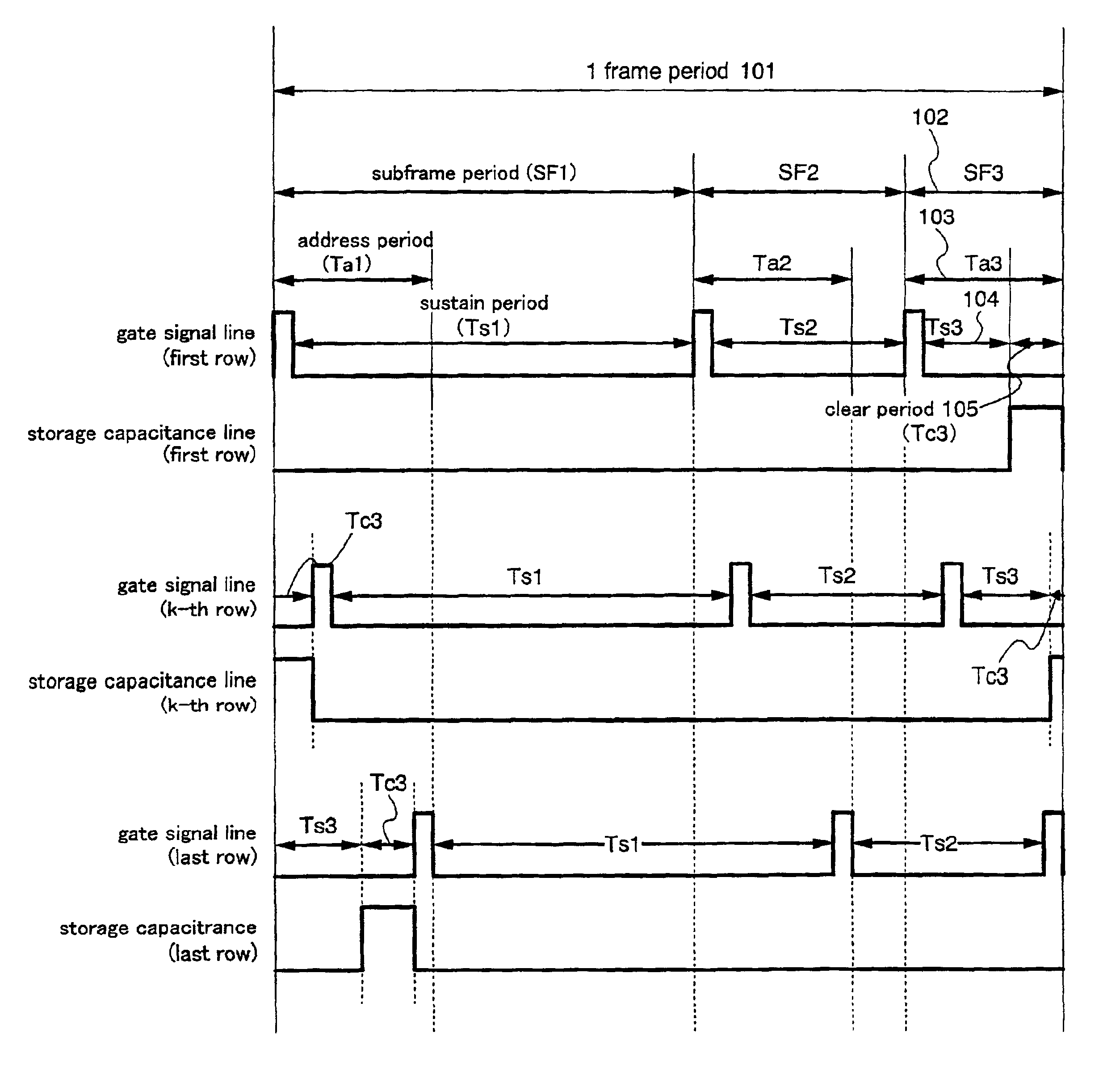
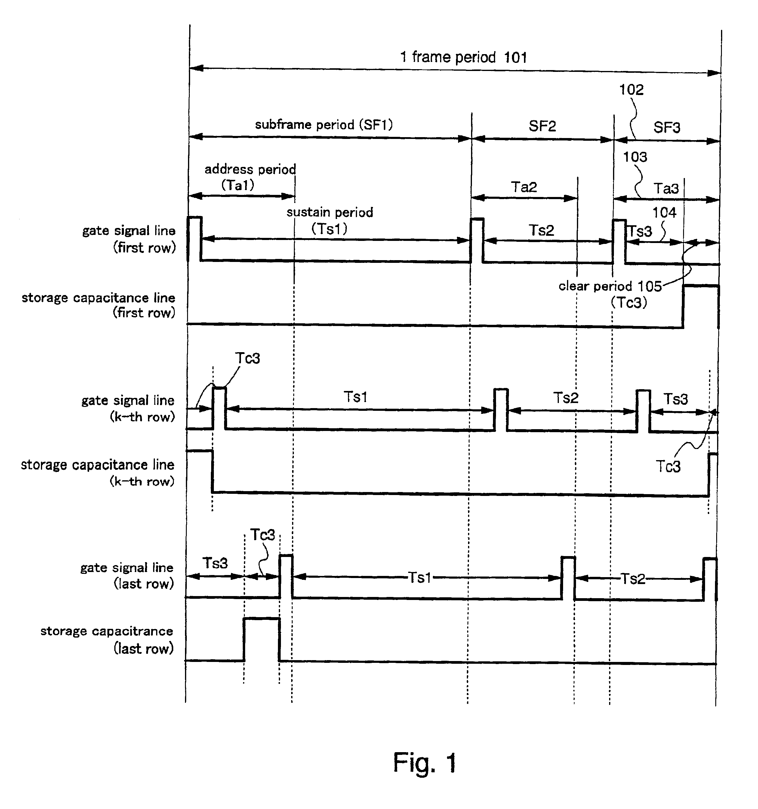
The actual driving method will be described using a timing chart. Discussed here is a driving method that uses digital gray scale and time gray scale in combination to obtain n bit gray scale display. For simplification, n is set to 3 here and display of 23=8 gray scales will be described. The circuit diagrams of FIGS. 20A and 20B are referred to again.

FIG. 1 is a timing chart of the electric potential of the gate signal line and of the storage capacitor line in the respective rows in this case. According to the circuit used in this embodiment, a switching TFT 2001 is a...

embodiment 2

Described in Embodiment 2 is a case in which the number of gray scales is larger than in Embodiment 1, and there are plural sustain (lights-on) periods each of which is shorter than an address (writing) period. The circuit here is the same as the one in Embodiment 1 and reference is again made to FIGS. 20A and 20B.

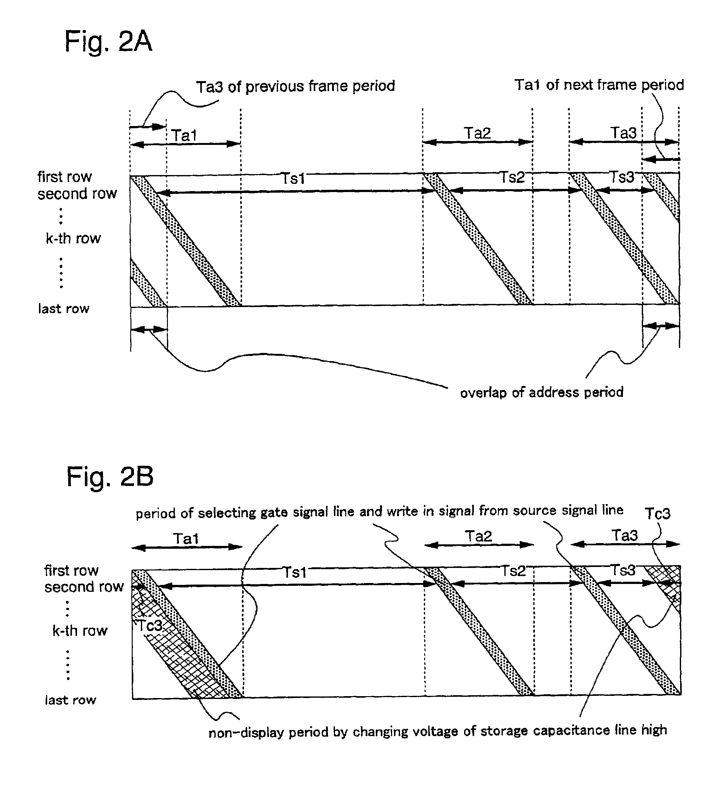
In this embodiment, display of 5 bit (25=32) gray scales is discussed. Similar to the case of 3 bit gray scale display, address (writing) periods Ta1 to Ta5 all have the same length and sustain (lights-on) periods Ts1 to Ts5 are set so as to satisfy Ts1:Ts2:Ts3:Ts4:Ts5=16:8:4:2:1. Out of all the sustain (lights-on) periods, Ts3, Ts4 and Ts5 are each shorter than an address (writing) period.

In a driving method in which the EL element 2003 starts to emit light immediately after writing of signals is completed, if the next address (writing) period is started after the end of a sustain (lights-on) period, address (writing) periods of different sub-frame periods partially overl...

embodiment 3

In Embodiment 3, the active layer of the n-channel TFT contains a source region, a drain region, a GOLD region, an LDD region, and a channel forming region, and the GOLD region overlaps with the gate electrode through the gate insulating film.

Further, there is not much need to worry about degradation due to hot carrier injection with the p-channel TFT of the CMOS circuit, and therefore LDD regions need not be formed in particular. It is of course possible to form an LDD region similar to that of the n-channel TFT, as a measure against hot carriers.

In addition, when using a CMOS circuit in which electric current flows in both directions in the channel forming region, namely a CMOS circuit in which the roles of the source region and the drain region interchange, it is preferable that LDD regions be formed on both sides of the channel forming region of the n-channel TFT forming the CMOS circuit, sandwiching the channel forming region. A circuit such as a transmission gate used in dot-s...


PUM


Abstract

To provide a novel driving method for driving an electronic device by using digital gray scale and time gray scale in combination, which secures high duty ratio, which can display an image normally even when a sustain period is shorter than an address period, and which is hardly affected by dulled signal waveform. In a sub-frame period (102) where a sustain period is shorter than an address period, a clear period (105) is squeezed in between completion of a sustain period (104) and start of an address period of the subsequent sub-frame period. The length of the sustain period (104) thus can be set without being limited by the length of an address period (103). This non-display period is provided by changing the electric potential of a storage capacitor line. Therefore, unlike the case where the non-display period is provided by changing the electric potential of a cathode wiring, the present invention is hardly affected by dulled signal waveform.

Description

BACKGROUND OF THE INVENTION1. Field of the InventionThe present invention relates to the structure of an electronic device. The invention particularly relates to a method of driving an active matrix electronic device having a thin film transistor (TFT) that is formed on an insulator and to an electronic device driven by the method.2. Description of the Related ArtEL displays have lately been attracting attention as a flat panel display to replace LCDs (liquid crystal displays), and researches are being actively made on the EL displays.Similar to LCDs that have roughly two types of driving methods with one being passive matrix type used in, e.g., STN-LCDs and the other being active matrix type used in, e.g., TFT-LCDs, EL displays also are driven by roughly two types of driving methods. One is passive matrix type and the other is active matrix type.In the case of the passive matrix type method, wirings to serve as electrodes are arranged above and below an EL element. A voltage is seq...

Claims


Application Information

Patent Timeline
IPC IPC(8): G09G3/20G09G3/32H05B44/00
CPCG09G3/2022G09G3/3258G09G3/2018G09G2300/0426G09G2310/061G09G2300/0861G09G2300/0876G09G2310/0262G09G2300/0842H10K59/8723H10K59/131H10K59/1213H10K59/1216H10K50/8428H10K59/1201G09G3/3266G09G2310/08
Inventor KIMURA, HAJIMETANADA, YOSHIFUMI
Owner SEMICON ENERGY LAB CO LTD
Why Eureka
Try Eureka