Transistor for active matrix display and a method for producing said transistor

a technology of active matrix and transistor, which is applied in the direction of transistors, semiconductor devices, electrical devices, etc., can solve the problems that no improvement would be expected from these studies on the charging time of pixels, and achieve excellent threshold voltage stability, high level of drive circuit integration, and high field effect mobility

Inactive Publication Date: 2011-01-04
CENT NAT DE LA RECHERCHE SCI +1
View PDF6 Cites 4 Cited by
  • Summary
  • Abstract
  • Description
  • Claims
  • Application Information

AI Technical Summary

Benefits of technology

[0009]The purpose of the invention is hence to remedy the shortcomings mentioned above and to propose a transistor for active matrix display having one or more of the following features and advantages: namely, a high field effect mobility, an excellent threshold voltage stability, a high level of drive circuit integration and a high duty ratio, offering a low cost transistor for pixel-charging devices used in active matrix displays.

Problems solved by technology

Therefore, no improvement would be expected from these studies on the charging time of pixels using said μc-Si:H thin film transistors and on the driving circuit integration.

Method used


Image

  • Transistor for active matrix display and a method for producing said transistor
  • Transistor for active matrix display and a method for producing said transistor
  • Transistor for active matrix display and a method for producing said transistor

Examples


example 1

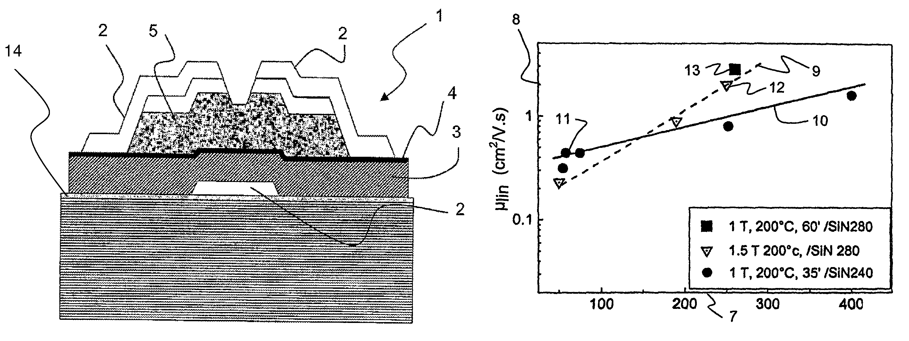
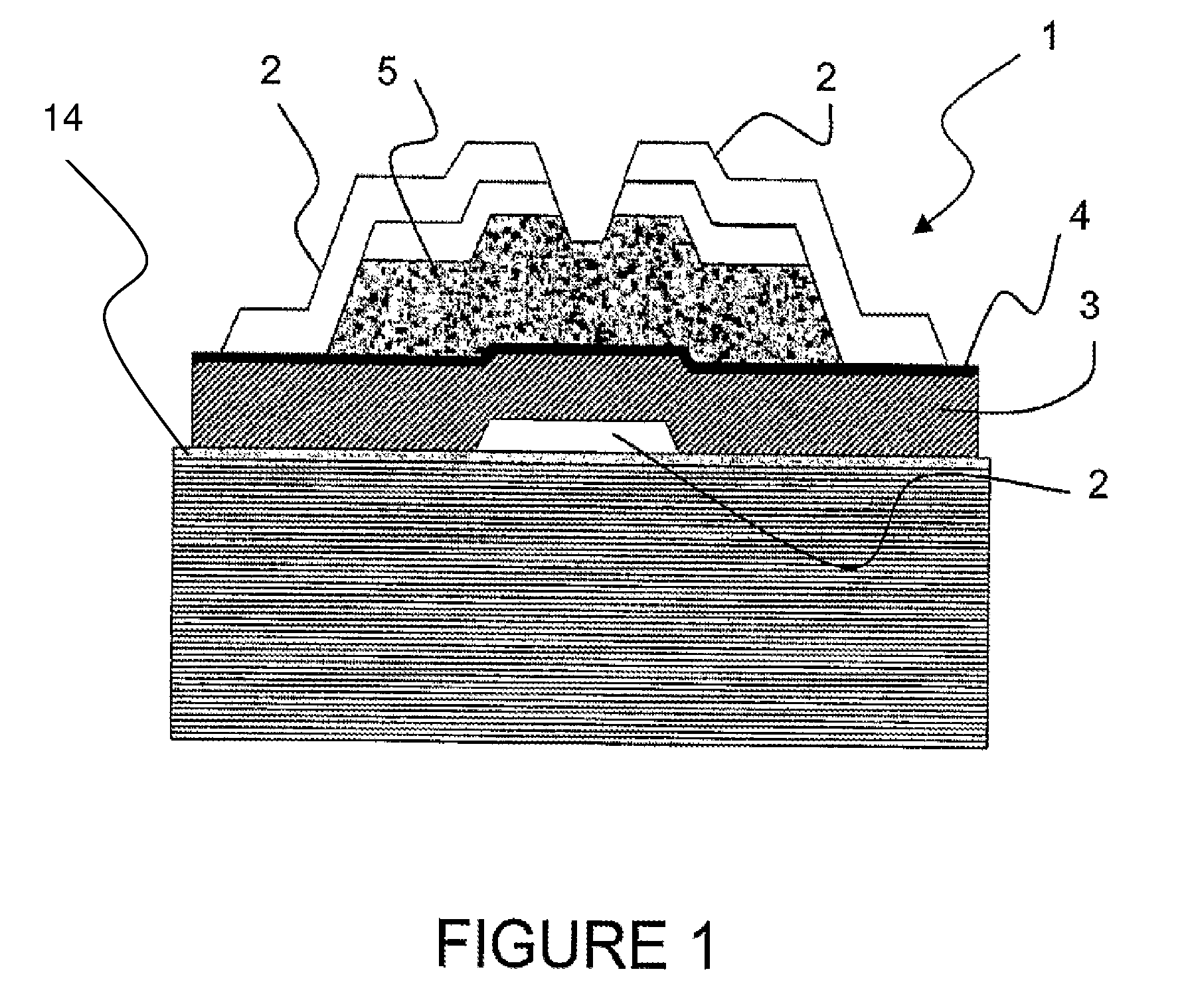
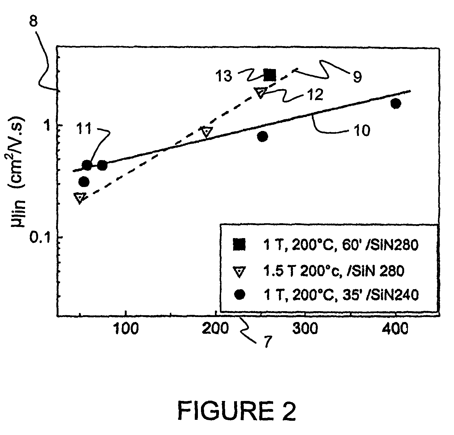
[0067]The method for producing a transistor 1 according to the invention has been first implemented to study a bottom gate thin film transistor produced from SiF4-Ar-H2 mixtures. FIG. 2 shows the experimental (circles, respectively inverted triangles) values obtained as a function of the “percolation thickness” (nm) 7 for the linear mobility (cm2V−1s−1) 8 of said μc-Si:H thin film transistor. The “percolation thickness” is a parameter which is defined as the thickness at which the crystalline fraction in the film reaches 100%. The dashed line 9 (respectively solid line 10) Is only shown to provide a guide line to the eye.

[0068]The circle values 11 were obtained for a μc-Si:H thin film formed by plasma deposition on a SiNx substrate under a total pressure of 1 Torr of SiF4-Ar-H2 mixtures and an RF power of 240 mW / cm2for 35 minutes. The inverted triangle values 12 were obtained for a μc-Si:H thin film formed by plasma deposition at a RF power of 280 mW / cm2 The pressure of said mixture...

example 2

[0070]FIG. 3 shows an atomic force microscopy (AFM) relief of a μc-Si:H thin film 5. The μc-Si:H thin film 5 was formed by submitting a SiNx thin film 3 to an Ar plasma and then to a SiF4-Ar-H2 mixture plasma treatment. The image extends laterally over an area of 5×5 μm2. Measurements of the thin film transistor realised with said μc-Si:H thin film show values for the linear mobility of the order of 0.02 cm2 / V.s. This AFM image clearly shows small crystallites 6 having a mean size less than 80 nm.

[0071]FIG. 4 shows an atomic force microscopy relief of a μc-Si:H thin film produced from a SiF4-Ar-H2 mixture. The μc-Si:H thin film was formed on a SiNx thin film submitted to a N2 treatment. The image extends laterally over an area of 2×2 μm2 Measurements of the thin film transistor realised with said μc-Si:H thin film show values for the linear mobility of the order of 3 cm2 / V.s. This AFM image clearly shows small crystallites having a mean size of the order of 400 nm.

[0072]The formatio...


PUM


Abstract

A transistor for active matrix display and a method for producing the transistor (1). The transistor (1) includes a microcrystalline silicon film (5) and an insulator (3). The crystalline fraction of the microcrystalline silicon film (5) is above 80%. According to the invention, the transistor (1) includes a plasma treated interface (4) located between the insulator (3) and the microcrystalline silicon film (5) so that the transistor (1) has a linear mobility equal or superior to 1.5 cm2V−1s−1, shows threshold voltage stability and wherein the microcrystalline silicon film (5) includes grains (6) whose size ranges between 10 nm and 400 nm. The invention concerns as well a display unit having a line-column matrix of pixels that are actively addressed, each pixel comprising at least a transistor as described above.

Description

[0001]This application is a Nation Stage Application of International Application PCT / EP2004 / 001107, filed Feb. 6, 2004.BACKGROUND OF THE INVENTION[0002]1. Field of the Invention[0003]The invention relates to a transistor for active matrix display, a display unit comprising the said transistor and a method for producing the said transistor.[0004]2. Description of Related Art[0005]Since the advent of the portables and the need for flat display panels, electronic displays implementing thin-film transistor technology and liquid crystals have experienced a phenomenal growth, to the point where full-colour displays have been realised that can compete with cathode ray tube displays. Amorphous silicon thin-film transistors are extensively used as pixel charging devices in active matrix liquid crystal displays, principally because of its application to large glass substrates, low cost and remarkable matching with the requirements of liquid crystal driving. Over the last decade, a rapidly gr...

Claims


Application Information

Patent Timeline
Patent Type & Authority Patents(United States)
IPC IPC(8): H01L21/00H01L21/336H01L29/786
CPCH01L29/66765H01L29/78603H01L29/78678
Inventor ROCA I CABARROCAS, PEREVANDERHAGHEN, REGISDREVILLON, BERNARD
Owner CENT NAT DE LA RECHERCHE SCI
Why Eureka
Try Eureka