Semiconductor device, display device, and electronic device

Active Publication Date: 2007-06-07
SEMICON ENERGY LAB CO LTD
View PDF17 Cites 120 Cited by
  • Summary
  • Abstract
  • Description
  • Claims
  • Application Information

AI Technical Summary

Benefits of technology

[0013] In view of the foregoing problems, it is an object of the invention to provide a display device with low power consumption and a high duty ratio. It is another object of

Problems solved by technology

When the duty ratio is low, the amount of current supplied to a light-emitting element through a driving transistor has to be increased; therefore, a voltage applied to the light-emitting element becomes higher, which results in high power consumption.
Further, since the light-emitting el

Method used


Image

  • Semiconductor device, display device, and electronic device
  • Semiconductor device, display device, and electronic device
  • Semiconductor device, display device, and electronic device

Examples


embodiment mode 1

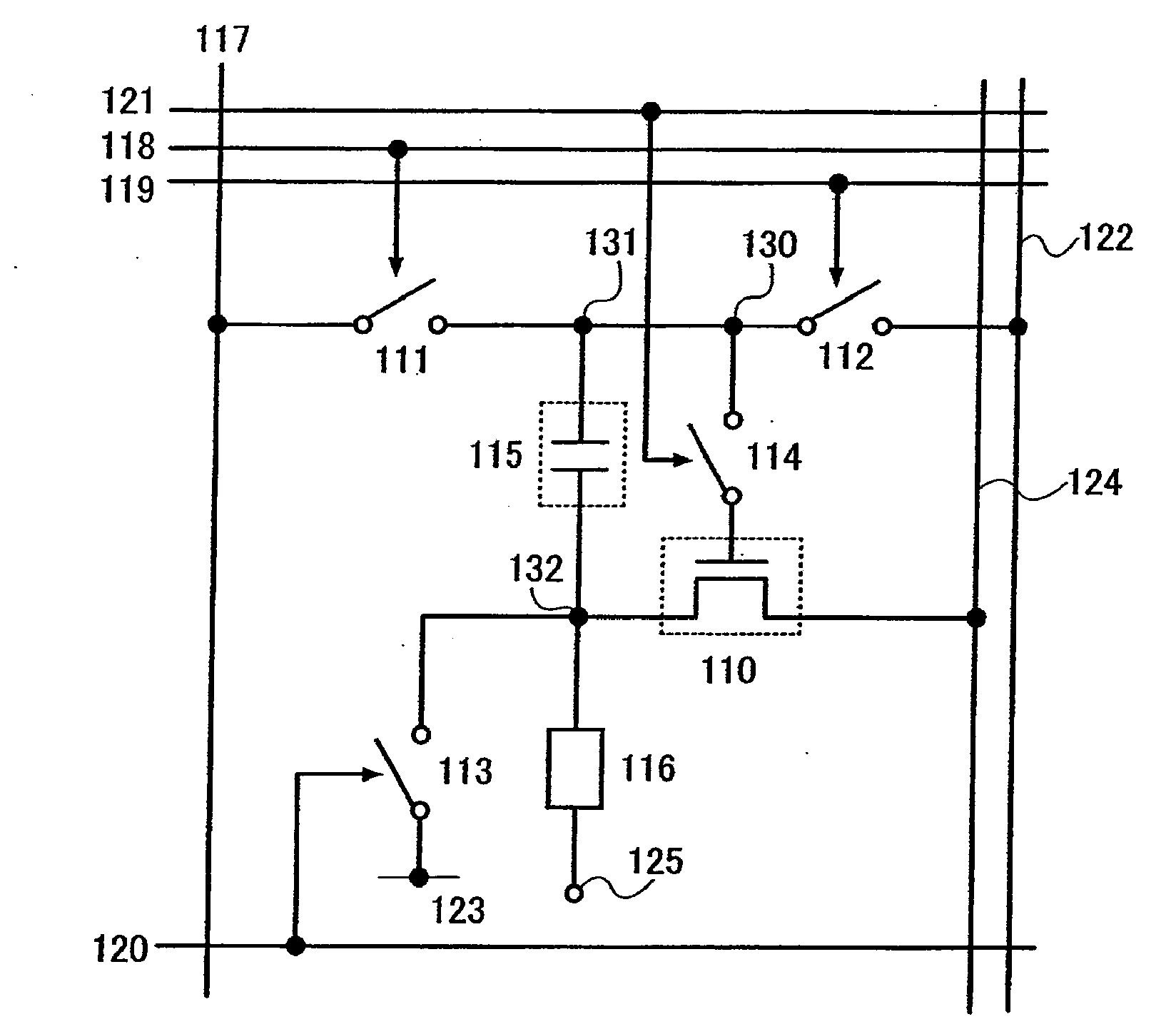
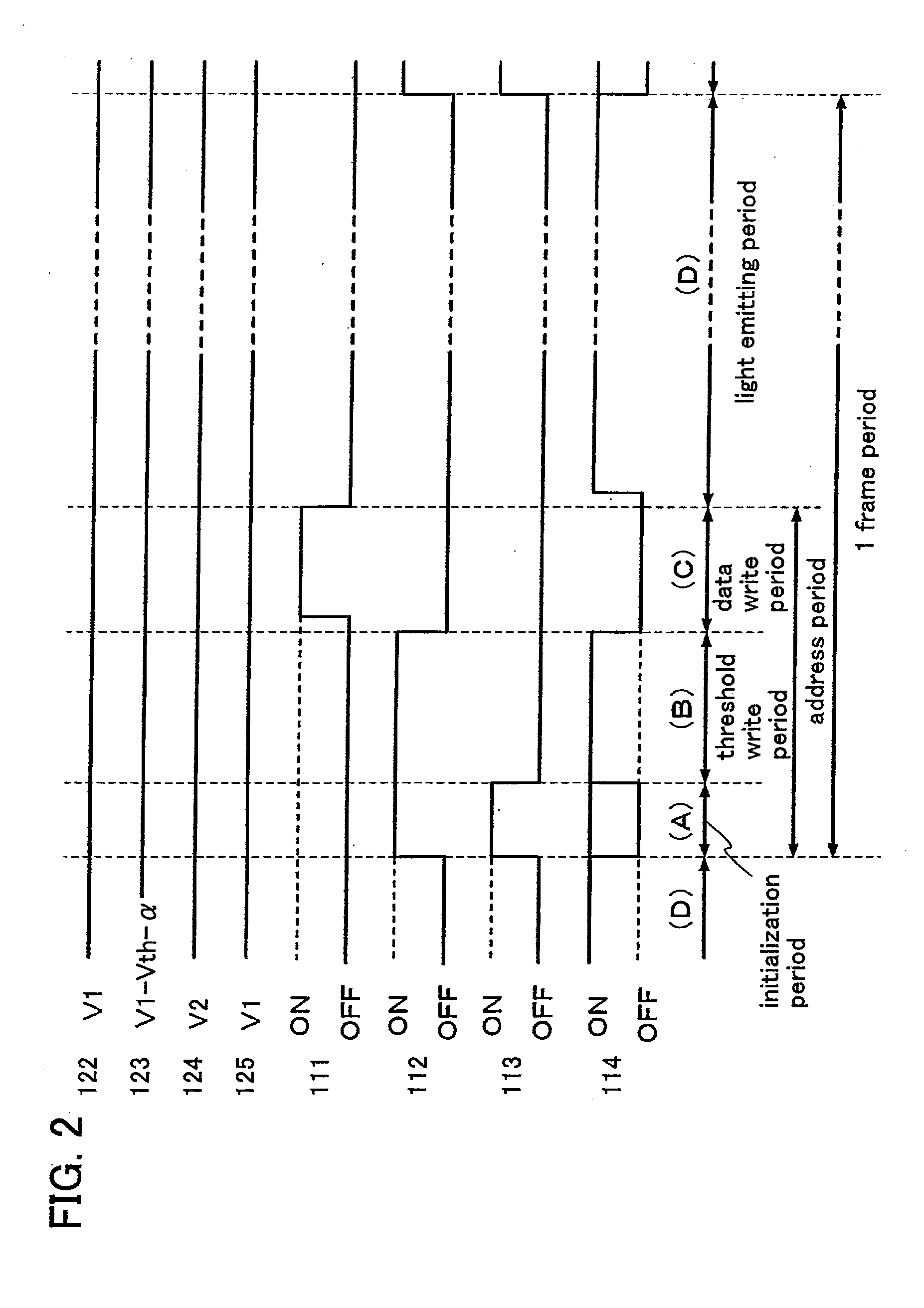
[0095] A basic configuration of a pixel of the invention is described with reference to FIG. 1. The pixel shown in FIG. 1 includes a transistor 110, a first switch 111, a second switch 112, a third switch 113, a fourth switch 114, a capacitor 115, and a light emitting element 116. The pixel is connected to a signal line 117, a first scan line 118, a second scan line 119, a third scan line 120, a fourth scan line 121, a first potential supply line 122, a second potential supply line 123, and a power supply line 124. In this embodiment mode, the transistor 110 is an n-channel transistor which is turned on when a gate-source voltage (Vgs) thereof exceeds the threshold voltage (Vth). In addition, a pixel electrode of the light emitting element 116 is an anode and an opposite electrode 125 thereof is a cathode. Note that the gate-source voltage of the transistor is represented by Vgs; the drain-source voltage, Vds; the threshold voltage, Vth; and a voltage accumulated in the capacitor, V...

embodiment mode 2

[0155] In this embodiment mode, a pixel with a different configuration from Embodiment Mode 1 is described with reference to FIG. 11. Note that portions common to this embodiment mode and the preceding embodiment mode are denoted by common reference numerals, and thus detailed description of the same portion or a portion having a similar function is omitted.

[0156] The pixel shown in FIG. 11 includes a transistor 110, a first switch 111, a second switch 112, a third switch 113, a capacitor 115, and a light emitting element 116. The pixel is connected to a signal line 117, a first scan line 118, a second scan line 119, a third scan line 120, a first potential supply line 122, a second potential supply line 123, and a power supply line 124.

[0157] A first electrode (one of a source electrode and a drain electrode) of the transistor 110 is connected to a pixel electrode of the light-emitting element 116; a second electrode (the other of the source electrode and the drain electrode) the...

embodiment mode 3

[0172] In this embodiment mode, a pixel having a different configuration from that in Embodiment Mode 1 is described with reference to FIGS. 16A to 16F. Note that portions common to FIGS. 1 and 16A through 16F are denoted by common reference numerals, and thus detailed description of the same portion or a portion having a similar function is omitted.

[0173] The pixel shown in FIG. 16A includes a transistor 110, a first switch 111, a second switch 112, a fourth switch 114, a capacitor 115, a light emitting element 116, and a rectifier element 1613. The pixel is connected to a signal line 117, a first scan line 118, a second scan line 119, a fourth scan line 121, a first potential supply line 122, a third scan line 1620, and a power supply line 124.

[0174] In the pixel shown in FIG. 16A, the rectifier element 1613 is used as the third switch 113 in FIG. 1, and a second electrode of the capacitor 115, a first electrode of a transistor 110, and a pixel electrode of the light emitting el...


PUM


Abstract

A display device includes a load, a transistor for controlling a current value supplied to the load, a capacitor, a first wiring, a second wiring, and first to fourth switches. Variations in the current value caused by variations in the threshold voltage of the transistor can be suppressed through the steps of: (1) holding the threshold voltage of the transistor in the storage capacitor, (2) inputting a potential in accordance with a video signal, and (3) holding a voltage that is the sum of the threshold voltage and the potential in accordance with the video signal, in the storage capacitor. Accordingly, a desired current can be supplied to the load such as a light emitting element.

Description

TECHNICAL FIELD [0001] The present invention relates to a semiconductor device having a function of controlling a current supplied to a load with a transistor, and a display device which includes a pixel formed using a current-drive display element whose luminance changes in accordance with signals, and a signal line driver circuit and a scan line driver circuit which drive the pixel. The invention also relates to a driving method of such a semiconductor device and display device. Further, the invention relates to an electronic device having the display device in a display portion. BACKGROUND ART [0002] In recent years, a self-luminous display device having a pixel formed using a light emitting element such as an electroluminescent (EL) element, i.e., a light emitting device has attracted attention. As a light emitting element used for such a self-luminous display device, an organic light emitting diode (OLED) and an EL element have attracted attention, which have been used for an E...

Claims


Application Information

Patent Timeline
IPC IPC(8): G09G3/30H05B44/00
CPCG09G3/3233G09G2300/0417G09G2300/0809G09G2300/0861H01L27/15G09G2320/0295G09G2320/043H01L27/12H01L27/13G09G2310/0251H01L21/02579H01L21/02576H01L2924/13069
Inventor KIMURA, HAJIME
Owner SEMICON ENERGY LAB CO LTD
Why Eureka
Try Eureka