Apparatus for attaching polarizing plate

a technology of polarizing plate and polarizing plate, which is applied in the direction of polarizing elements, instruments, chemistry apparatus and processes, etc., can solve the problems of high manufacturing cost, many critical problems in conventional manufacturing processes, so as to reduce the time for enhance the productivity of manufacturing liquid crystal display devices

Inactive Publication Date: 2005-02-01
SAMSUNG DISPLAY CO LTD
View PDF5 Cites 24 Cited by
  • Summary
  • Abstract
  • Description
  • Claims
  • Application Information

AI Technical Summary

Benefits of technology

According to the present invention, a polarizing plate is attached onto an assembled substrate on which at least one liquid crystal display unit cells are formed, the at least one liquid crystal display unit cells are separated from the assembled substrate, a liquid crystal display panel is manufactured, and a driving module is installed on the liquid crystal display panel, so that the time for manufacturing the liquid crystal display device are reduced and the productivity of manufacturing the liquid crystal display device is enhanced.

Problems solved by technology

However, the conventional manufacturing processes has some critical problems.
However, the greater the number of the equipment is, the higher is the manufacturing cost.
Further, the conventional manufacturing processes have many problems.
A first problem occurs in the rubbing process.
The particles may induce failures during the rubbing process.
Therefore, the conventional rubbing process cannot be successfully performed and the efficiency of manufacturing the liquid crystal display device is lowered.
Therefore, defects of the alignment grooves are seldom detected, when the alignment grooves are already formed.
The defects of the alignment grooves may be detected in the reliability test of the liquid crystal display device after the liquid crystal display device is completely manufactured.
The liquid crystal display device having a defect of the alignment groove lowers image display quality.
A second problem occurs after the assembled substrate is manufactured.
A fourth problem occurs in the module process.
Therefore, much time is required so as to attach the polarizing plate onto the assembled substrate.
However, it is hard to detect the defect of the liquid crystal display device unit cell before cutting off the assembled substrate.
When a polarizing plate is attached onto a defective liquid crystal display unit cell, the polarizing plate is wasted.

Method used


Image

  • Apparatus for attaching polarizing plate
  • Apparatus for attaching polarizing plate
  • Apparatus for attaching polarizing plate

Examples


first embodiment

<First Embodiment of a Non-Contact Type Alignment of Liquid Crystal Molecules>

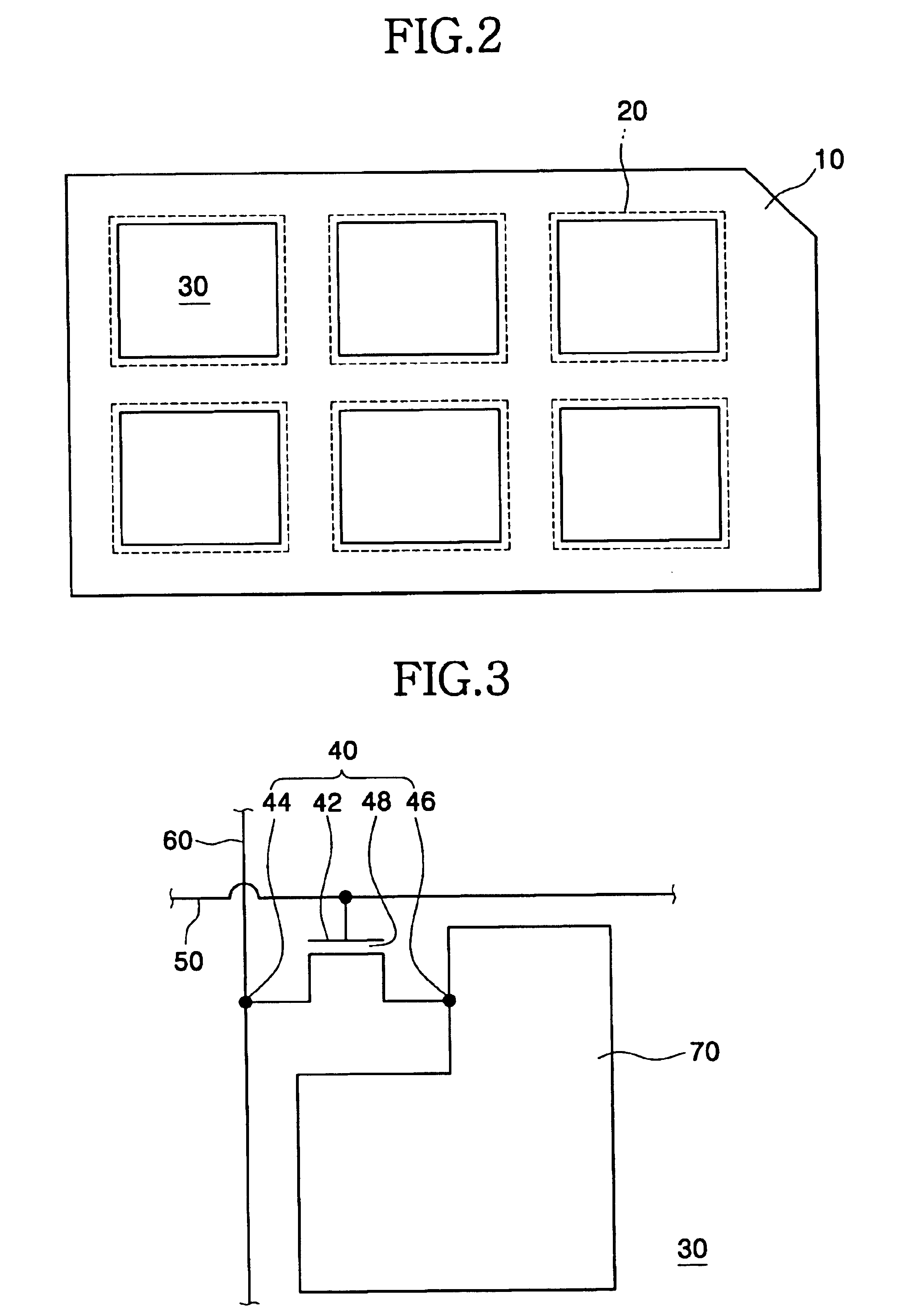
In order to align liquid crystal molecules on the thin film transistor unit cell 30 of FIG. 2 or on the color filter unit cell 100 of FIG. 5, an alignment film and an atomic beam to be applied to the alignment film are needed.

FIG. 7 is a cross-sectional view showing an alignment film formed on the first mother substrate or the second mother substrate according to the first exemplary embodiment.

Referring to FIG. 7, an alignment film 130 includes a diamond-like-carbon thin film (DLC film) formed on surfaces of the thin film transistor unit cell and on the color filter unit cell. The alignment film 130 may include SiO2, Si3N4 and TiO2 aside from the diamond-like-carbon thin film.

Hereinafter, the diamond-like-carbon thin film is referenced by the reference numeral 130.

The diamond-like-carbon thin film 130 is used as an alignment film because the diamond-like-carbon thin film 130 has a carbon-carbon double...

second embodiment

<Second Embodiment of a Non-Contact Type Alignment of Liquid Crystal Molecules>

FIG. 13 is a flow chart showing a method of aligning liquid crystal by a non-contact method according to a second exemplary embodiment.

In previous procedure, the diamond-like-carbon thin film having a carbon-carbon double bond is formed on the first substrate 10 having the thin film transistor unit cell 30 of FIG. 2 or on the second substrate 80 having the color filter unit cell 100 of FIG. 5. The diamond-like-carbon thin film is formed via Chemical Vapor Deposition (CVD).

Referring to FIG. 13, the atomic beam collides with the diamond-like-carbon thin film, so that a polarized functional group for aligning liquid crystal molecules is generated (step S225).

FIG. 14 is a flow chart showing a method of generating a polarized functional group in the diamond-like-carbon thin film according to the second exemplary embodiment.

Referring to FIG. 14, a first ion beam is generated and accelerated toward the diam...

third embodiment

<Third Embodiment of a Non-Contact Type Alignment of Liquid Crystal Molecules>

FIG. 16 is a flow chart showing a process of introducing a hydrogen ion into the polarized functional group according to a third exemplary embodiment of the present invention.

Deionized water is supplied to the surface of the diamond-like-carbon thin film in order that hydrogen ion (H+) is combined with the sub-chain (step S233).

Then, ultra-violet ray is irradiated onto the surface of the diamond-like-carbon thin film in order that the hydrogen ion (H+) is combined with the sub-chain (step S234).

When the ultra-violet ray is irradiated on the deionized water, two hydrogen ions and one oxygen ion are generated as shown in the following chemical formula.

<Chemical Formula 1>

H2O−>2H++O−2

The hydrogen ion (H+) dissociated by the ultra-violet ray is combined with the sub-chain to form a C—H bond.

When the hydrogen ion (H+) is combined with the sub-chain formed in the diamond-like-carbon thin film in which ...


PUM

PropertyMeasurementUnit
sizeaaaaaaaaaa
temperatureaaaaaaaaaa
angleaaaaaaaaaa

Abstract

The apparatus of attaching a polarizing plate includes a base body, a first cutting out module, a first protection sheet strip module and a first polarizing plate attaching module. The first cutting out module cuts out a first polarizing plate from a first mother polarizing plate. The first cutting out module is disposed on the base body. The first protection sheet strip module strips a first protection sheet from the first polarizing plate. The first polarizing plate is stripped off the first protection sheet to be a first stripped polarizing plate. The first protection sheet strip module is disposed on the base body. The first polarizing plate attaching module attaches the first stripped polarizing plate to a first face of a liquid crystal display unit cell of an assembled substrate. The first polarizing plate attaching module is disposed on the base body.

Description

CROSS-REFERENCE TO RELATED APPLICATIONSThis application relies for priority upon Korean Patent Application No.2002-78499 filed on Dec. 10, 2002, the contents of which are herein incorporated by reference in its entirety.BACKGROUND OF THE INVENTION1. Field of the InventionThe present invention relates to an apparatus for attaching a polarizing plate, and more particularly to an apparatus for attaching a polarizing plate on an assembled substrate that include a plurality of liquid crystal display unit cells.2. Description of the Related ArtIn general, a liquid crystal display device is lighter and smaller than other display devices comparatively. The liquid crystal display devices are manufactured via many manufacturing processes.A first process for manufacturing the liquid crystal display device includes a forming of thin film transistor (tft) unit cells on a first mother substrate and a forming of color filter unit cells on a second mother substrate. One example of the first process...

Claims


Application Information

Patent Timeline
Patent Type & Authority Patents(United States)
IPC IPC(8): G02F1/1337G02F1/13G02F1/1333G02F1/1335G02B5/30
CPCG02F1/1333G02F1/13378G02F1/1309G02F1/133351G02F1/133528Y10T156/1077Y10T156/1339Y10T156/12Y10T156/1751Y10T156/1062Y10T156/1092Y10T156/1074G02F1/13
Inventor CHOO, DAE-HOPARK, CHUN-BOKHER, SEUNG-HEE
Owner SAMSUNG DISPLAY CO LTD
Why Eureka
Try Eureka