Semiconductor device with uneven metal plate to improve adhesion to molding compound

a technology of metal plate and molding compound, which is applied in the direction of semiconductor devices, semiconductor/solid-state device details, electrical apparatus, etc., can solve the problems of unsuitable high-current package, unsuitable for high-current use, and increase the fabrication cost. , to achieve the effect of further improving the oxidation prevention effect of metal pla

Inactive Publication Date: 2005-02-01
RENESAS ELECTRONICS CORP
View PDF38 Cites 61 Cited by
  • Summary
  • Abstract
  • Description
  • Claims
  • Application Information

AI Technical Summary

Benefits of technology

By composing such a constitution, since the surface of the metal plate is roughened, the adhesion strength between the metal plate and the molding resin is improved and the closed property (sealed property) provided by the molding resin is improved and the reliability of the semiconductor device is improved.
By composing such a constitution, the oxidation preventive effect of the metal plate is further improved.

Problems solved by technology

However, by the wire bonding method using a costly thin metal wire such as a gold wire or the like, problems are caused.
Not only is the fabrication cost considerably increased but also disconnection takes place in the thin metal wire to make the package unsuitable for high electric current use.
However, in a plastic package in which electrodes of a semiconductor chip and the lead terminals of wiring materials are electrically connected by a metal plate, there exist the following problems.
Because the semiconductor device is repeatedly subjected to temperature alteration, the bonding of the metal plate and the molding resin ocassionally becomes broken, causing separation of the metal plate from the resin.
Then, water and a corrosive gas may penetrate the semiconductor chip through the parted interfaces to cause corrosion of the semiconductor chip.
As a result, the reliability of the semiconductor device is lowered.
This adversely affects the reliability of the semiconductor device, as it is deteriorated by the water and gas penetration.
Further, although in some cases, a solder paste and a resin type conductive paste are used for bonding the lead terminals and the metal plate, the solder paste and the conductive paste sometimes flow out of the bonding range of the metal plate and the lead terminals.
In the case where the solder paste and the conductive paste flow from the lead terminals in the extended direction of the leads and are spread from the lead terminals to the package outer circumference position and to the peripheral part of the package outer circumference, the conductive paste and the like decrease the adhesion strength of the molding resin and cause the separation of the molding resin.
As a result, water and the gas may easily penetrate the semiconductor chip from the outside and cause corrosion of the semiconductor chip, resulting in reduced reliability of the semiconductor device.

Method used


Image

  • Semiconductor device with uneven metal plate to improve adhesion to molding compound
  • Semiconductor device with uneven metal plate to improve adhesion to molding compound
  • Semiconductor device with uneven metal plate to improve adhesion to molding compound

Examples


embodiment 2

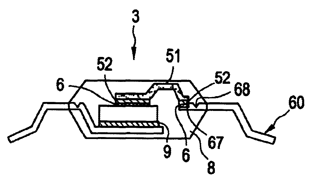
Next, an embodiment 2 of a semiconductor device 4 of the present invention will be described with reference to FIGS. 9A and 9B and FIGS. 10A to 10C. FIGS. 9A and 9B are illustrations showing the semiconductor device 4 of the embodiment 2 of the present invention and FIG. 9A is a plane view and FIG. 9B is a cross-section cut along the VIII-VIII′ line in FIG. 9A. FIGS. 10A to 10C are illustrations showing a copper plate 56 to be employed for the semiconductor device 4 of the embodiment 2 of the present invention. FIG. 10A is a plane view, FIG. 10B is a cross-section cut along the IX-IX′ line in FIG. 10A, and FIG. 10C is the bottom FIG.

The semiconductor device 4 of the embodiment 2 has the same constitution as that of the semiconductor device 3 of the embodiment 1. However, it is different in the point that claw parts 58 are formed in the copper plate 56.

Similar to the copper plate 51 in the embodiment 1, the copper plate 56 is plated with silver plating 57a, 57b. As illustrated in FIG...


PUM

PropertyMeasurementUnit
surface roughnessaaaaaaaaaa

Abstract

The present invention provides a semiconductor device whose reliability is improved by improving the adhesion strength of a metal plate or connecting chip, said plurality of electrodes and a lead frame with a molding resin. Further, the semiconductor device of the present invention prevents flow out of a conductive joining material to be employed for joining a lead terminal and the metal plate other than the joining range of the metal plate and the lead terminal, and mounts the metal plate at high precision. In a semiconductor device (a plastic package) in which a source electrode of a semiconductor chip and source terminal of a lead frame are electrically connected by a copper plate and sealed by a resin, the surface of the copper plate is roughened to improve the adhesion strength to a molding resin. Further, a stepped part is formed in the source terminal to prevent a conductive paste from flowing out. The structure is so formed as to fit claw parts in the lead frame.

Description

BACKGROUND OF THE INVENTION1. Field of the InventionThe present invention relates to a semiconductor device sealed with a resin, that is, a plastic package, and more particularly to a plastic package of which electrodes of a semiconductor chip and lead terminals are electrically connected to each other by a metal plate such as copper. The present application is based on Japanese Patent Application No. 264083 / 2000 and Japanese Patent Application No. 013869 / 2001, the disclosures of which are incorporated herein by reference.2. Description of the Related ArtA semiconductor device sealed with a resin, that is, a plastic package, comprises a semiconductor chip (also called a pellet or a die), wiring materials forming outer terminals such as a lead frame, and a molding resin for sealing the semiconductor chip bonded to the wiring materials and inner leads.Examples of the wiring materials are a tape carrier (a film carrier), a printed circuit plate, and the like other than a lead frame. As...

Claims


Application Information

Patent Timeline
Patent Type & Authority Patents(United States)
IPC IPC(8): H01L23/495H01L23/48H01L21/60H01L23/28
CPCH01L23/49524H01L23/49548H01L23/49562H01L24/35H01L24/36H01L24/40H01L24/45H01L24/48H01L2224/48639H01L2224/48644H01L2224/48624H01L2924/01023H01L2924/01006H01L2924/01005H01L2924/13091H01L2924/014H01L2924/01088H01L2924/01082H01L2924/01079H01L2924/01078H01L2924/01051H01L2924/01047H01L2924/01033H01L2924/01029H01L2924/01028H01L2924/01013H01L2924/01004H01L2224/73265H01L2224/05001H01L2224/05073H01L2224/05624H01L2224/05639H01L2224/05644H01L2224/32225H01L2224/32245H01L2224/45144H01L2224/48091H01L2224/48247H01L2224/73221H01L2924/00014H01L2924/00H01L2924/351H01L2924/181H01L2224/40095H01L2224/40245H01L2224/37147H01L2224/3754H01L24/37H01L2224/371H01L2224/8485H01L2224/84385H01L2224/05553H01L2224/0603H01L2224/3716H01L24/84H01L2924/00012H01L2224/43H01L23/495
Inventor NAKAJIMA, YOSHIHIROFUKUIZUMI, AKIRA
Owner RENESAS ELECTRONICS CORP
Why Eureka
Try Eureka