Light emitting diode

a technology of light-emitting diodes and diodes, which is applied in the direction of discharge tubes luminescnet screens, electric discharge lamps, lighting and heating apparatus, etc., can solve the problems of reducing the luminous efficacy, affecting the luminous efficacy of the assembled light-emitting diodes, and unable to eliminate the air layer, so as to achieve the effect of improving the luminous efficacy and ensuring the stable emission performance of the assembled light-

Inactive Publication Date: 2005-02-01
AVAGO TECH WIRELESS IP SINGAPORE PTE
View PDF10 Cites 141 Cited by
  • Summary
  • Abstract
  • Description
  • Claims
  • Application Information

AI Technical Summary

Benefits of technology

Consequently, the present invention presents a light-emitting diode having a relatively simple structure but with which optical properties (uniformity of color, flux distribution properties) are good, there are no fluctuations in emission color between products, and efficient emission performance is obtained, as well as a method for producing this light-emitting diode. Yet another object of the present invention is to present a high-performance light-emitting diode as previously described by a relatively simple and inexpensive production process.
A fluorescent material is applied to the surface of the convex inner face. Various printing or application methods used in the past can be employed for this application. By means of these methods, the thickness and the amount of the fluorescent material layer can be controlled and therefore, stable emission performance of the assembled light-emitting diode can be guaranteed.
Resin material is introduced inside the cup part prior to the process, whereby the lens member is attached to this base. Only a pre-determined amount of resin material is introduced into the cup, but there can be some variation in the amount that is introduced between products, particularly when multiple products are being produced. Then, when the lens member is attached, the inner convex face comes into contact with the resin material, pushing this resin material, and as a result, the resin material is deformed and part of it is moved. The lens member has a groove extending from the position of the inner convex face toward the outer rim and when the lens member engages with the cup part, some of the resin material is pushed to the convex inner face and moves so that it makes its way into this groove. Thus, the clearance into which air makes its way is not made between the convex inner face and the resin material and consequently, light from the light-emitting diode is not reflected at the interface between the convex inner face and resin material and luminous efficacy is improved.

Problems solved by technology

A problem with this type of light-emitting diode is that a clearance or gap can be formed when air makes its way in between the lens plate and the filler and therefore, the luminous efficacy drops due to the effect of this air layer.
It is all but impossible to eliminate the air layer when filler is introduced onto such a small surface area inside a cup and the lens plate is placed on top during the production process.
Nevertheless, as shown by the latter of the above-mentioned Patent Publications, using this type of process complicates production process and increases the cost of the product.
Moreover, another problem exists relating to wavelength conversion by the fluorescent material.
Nevertheless, this structure can produce irregularities in the light that is radiated to the outside due to the effect of differences in optical light paths emitted in each direction from the light-emitting diode chip, or a difference in the distribution of the fluorescent material.
Moreover, fluctuations in the emission color between products are relatively large and there are cases in which these cause inconveniences, depending on the purpose for which the product is used.

Method used


Image

  • Light emitting diode
  • Light emitting diode
  • Light emitting diode

Examples


Embodiment Construction

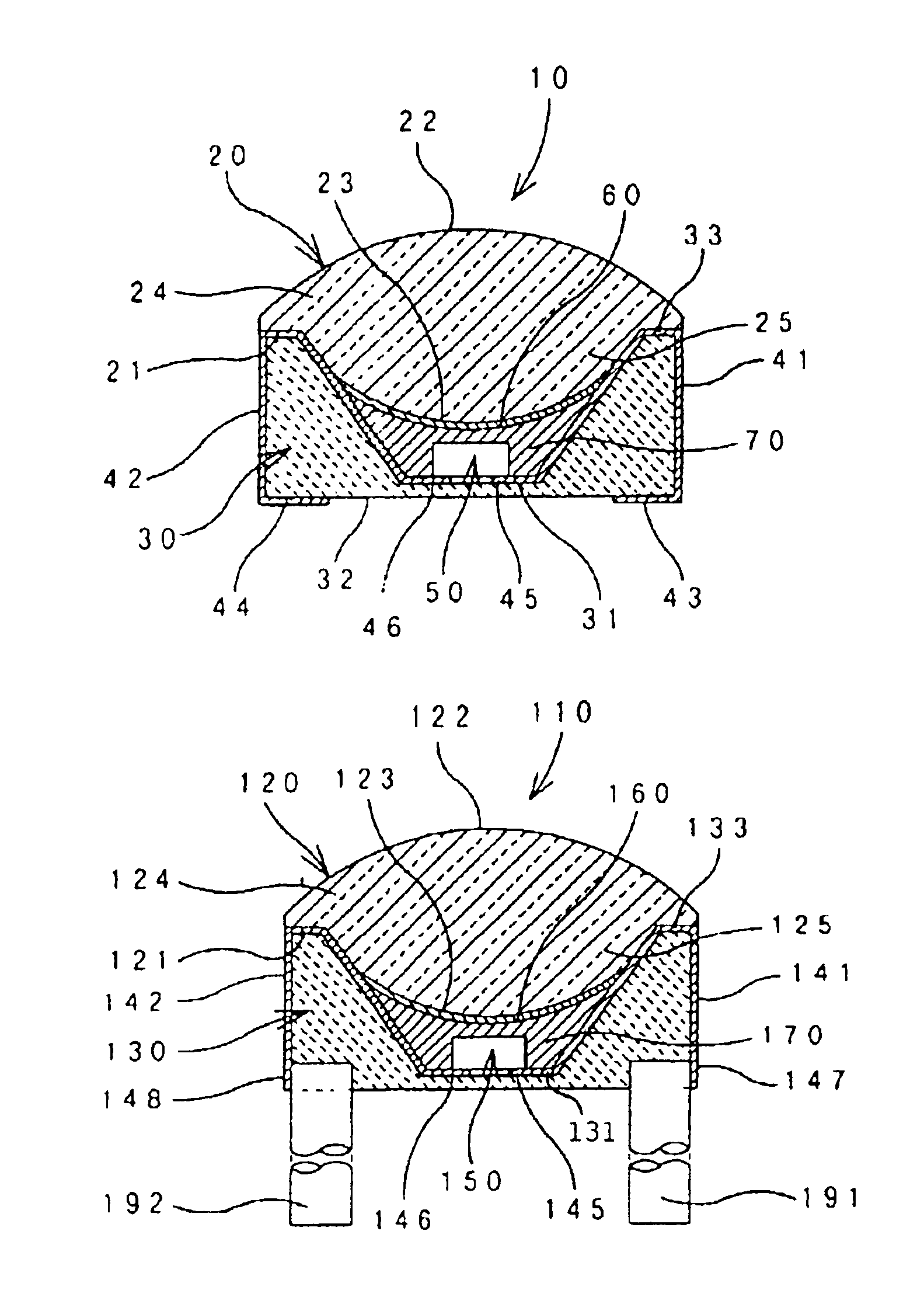
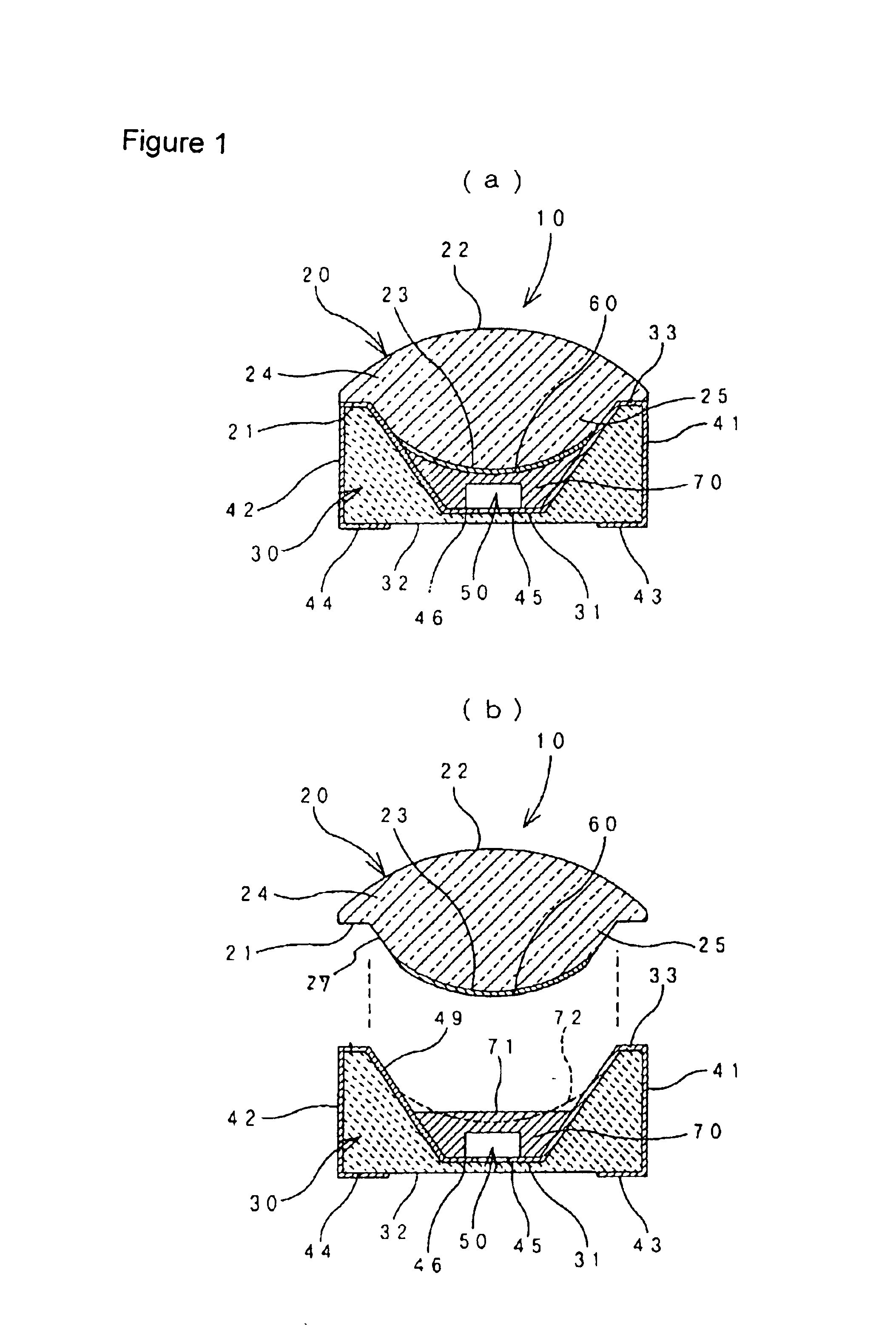
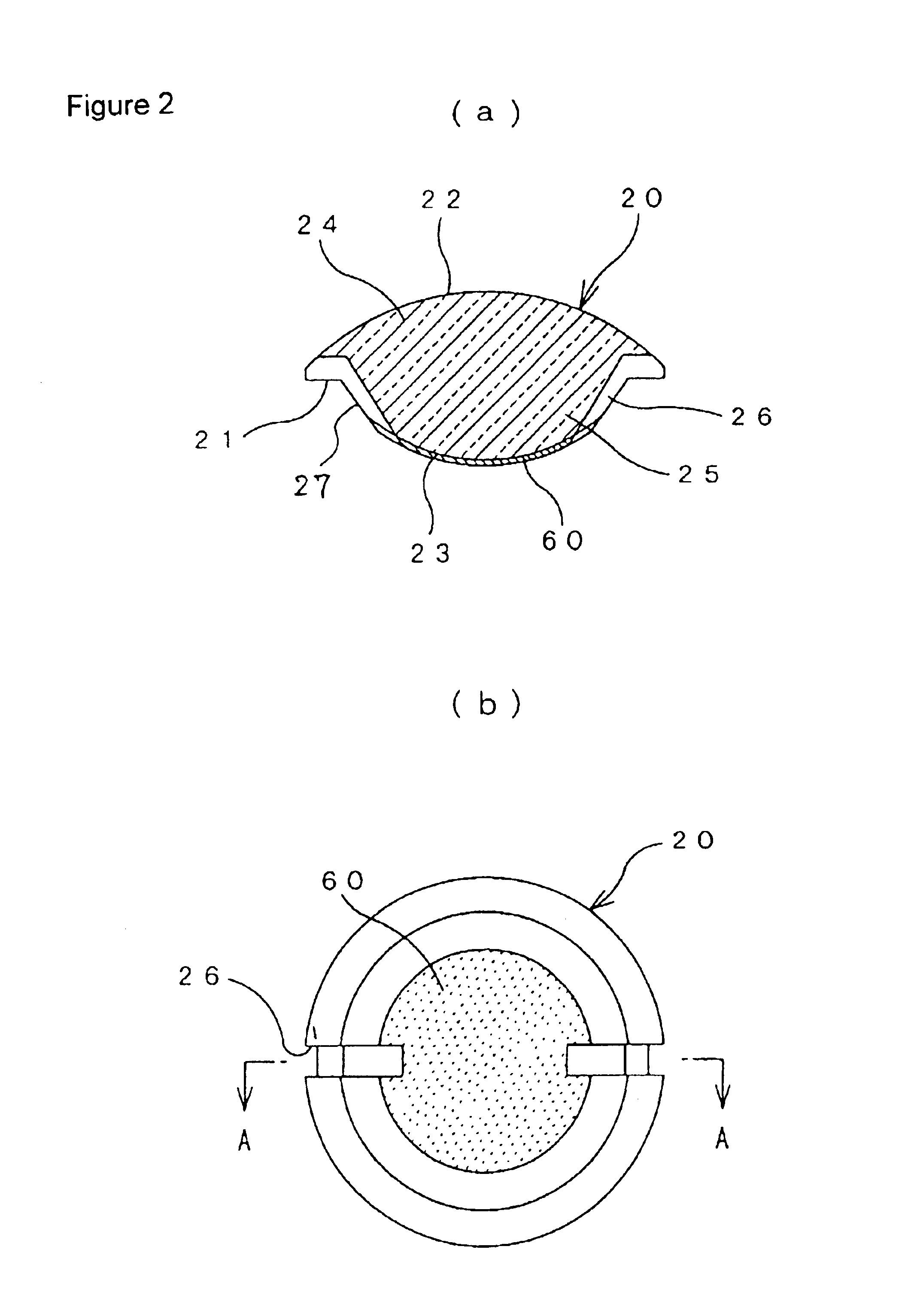
Light-emitting diodes and methods for their production that are preferred embodiments of the present invention will now be described in detail while referring to the attached drawings. FIG. 1 is a cross-section describing the light-emitting diode that is the first preferred embodiment of the present invention, with (a) showing the state when assembly is completed and (b) showing this state before assembly. FIG. 2 is a Fig. showing the structure of the lens member used in the light-emitting diode that is the first preferred embodiment. (a) is a bottom view and (b) is a cross-section along line A—A in (a).

Light-emitting diode 10, which is the first preferred embodiment, has light-emitting diode chip 50, base 30 that holds this chip, and lens member 20 set up on base 30. base 30 comprises cup part 31 with a concave structure, and light-emitting diode chip 50 is held and mounted inside this cup. Base 30 is worked into a pre-determined shape by grinding a ceramic material or molding a pl...


PUM


Abstract

A light-emitting diode with no fluctuations in optical properties and good sealing properties, and a simple production method for producing this light-emitting diode. The light-emitting diode has a base comprising a cup part on which the light-emitting diode is placed, a resin material introduced into cup part, and a lens member placed on top of a cup for focusing light emitted by a light-emitting diode chip. A layer of fluorescent material, which converts the wavelength of at least some of the light from the light-emitting diode chip, is applied to the inner convex face of the lens member. When the lens member is attached to the base, the inner convex face deforms the resin material and air and excess resin material can be pushed to the outside.

Description

BACKGROUND OF THE INVENTION1. Field of the InventionThe present invention pertains to a light-emitting diode, which is a light-emitting diode device comprising a light-emitting diode chip, particularly with which at least part of the light is converted in wavelength by a fluorescent material, making it possible to produce emission in a color that is different from the emission color of the light-emitting diode chip, for instance, white.2. Description of the Related ArtA conventional example of a light-emitting diode of this type is described, for instance, in Japanese Patent Publication No. 8(1996)-320,656 and Japanese Patent Publication No. 11(1999)-251,640. According to the former document, the light-emitting diode device has a printed wiring board and a mask plate made of rubber or resin on top of this, and part of this mask plate comprises a cup that reflects light. The light-emitting diode chip is mounted on the inside of this cup. Light-transmitting filler is introduced and ha...

Claims


Application Information

Patent Timeline
Patent Type & Authority Patents(United States)
IPC IPC(8): H01L33/00H01L33/50H01L33/56H01L23/28H01L33/58H01L33/62
CPCH01L33/507H01L33/58Y10S362/80H01L2924/0002H01L2924/00
Inventor TAKEKUMA, AKIRA
Owner AVAGO TECH WIRELESS IP SINGAPORE PTE
Why Eureka
Try Eureka