Phosphor-coated light emitting diodes including tapered sidewalls, and fabrication methods therefor

a light-emitting diode and phosphor-coated technology, applied in the direction of basic electric elements, electrical equipment, semiconductor devices, etc., can solve the problems of difficult to maintain the effectiveness of shaping techniques, difficult to use conventional techniques for light extraction, and difficult to use thick p-type window layers, etc., to achieve more uniform phosphor-containing coatings

Inactive Publication Date: 2005-02-08
CREELED INC
View PDF68 Cites 357 Cited by
  • Summary
  • Abstract
  • Description
  • Claims
  • Application Information

AI Technical Summary

Benefits of technology

Light emitting diodes according to some embodiments of the invention include a substrate having first and second opposing faces, and a diode region on the first face. The sidewall(s) of the light emitting diode extend at an oblique angle, rather than a 90° angle, from the second face towards the first face. In some embodiments, the oblique angle is an obtuse angle. In some embodiments, the oblique sidewall may extend from the second face to adjacent the diode region. A conformal phosphor-containing layer is included on at least a portion of the oblique sidewall. In other embodiments, the phosphor-containing layer is also included on the second face. According to some embodiments of the invention, by providing an oblique sidewall adjacent the second face, more uniform phosphor-containing coatings may be obtained compared to light emitting diodes that have a vertical (orthogonal) sidewall adjacent the second face.

Problems solved by technology

Unfortunately, the effectiveness of these shaping techniques may not be maintained as the chip dimensions are scaled up for higher power / intensity and / or other applications.
In such silicon carbide LEDs and / or gallium nitride LEDs on silicon carbide, it may be difficult to use conventional techniques for light extraction.
For example, it may be difficult to use thick p-type window layers because of the relatively low growth rate of gallium nitride.
Also, although such LEDs may benefit from the use of Bragg reflectors and / or substrate removal techniques, it may be difficult to fabricate a reflector between the substrate and the gallium nitride diode region and / or to remove at least part of the silicon carbide substrate.
The coating of a phosphor on an LED may further complicate light extraction problems.

Method used


Image

  • Phosphor-coated light emitting diodes including tapered sidewalls, and fabrication methods therefor
  • Phosphor-coated light emitting diodes including tapered sidewalls, and fabrication methods therefor

Examples


Embodiment Construction

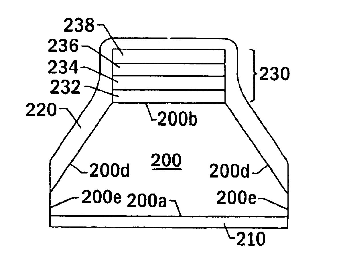
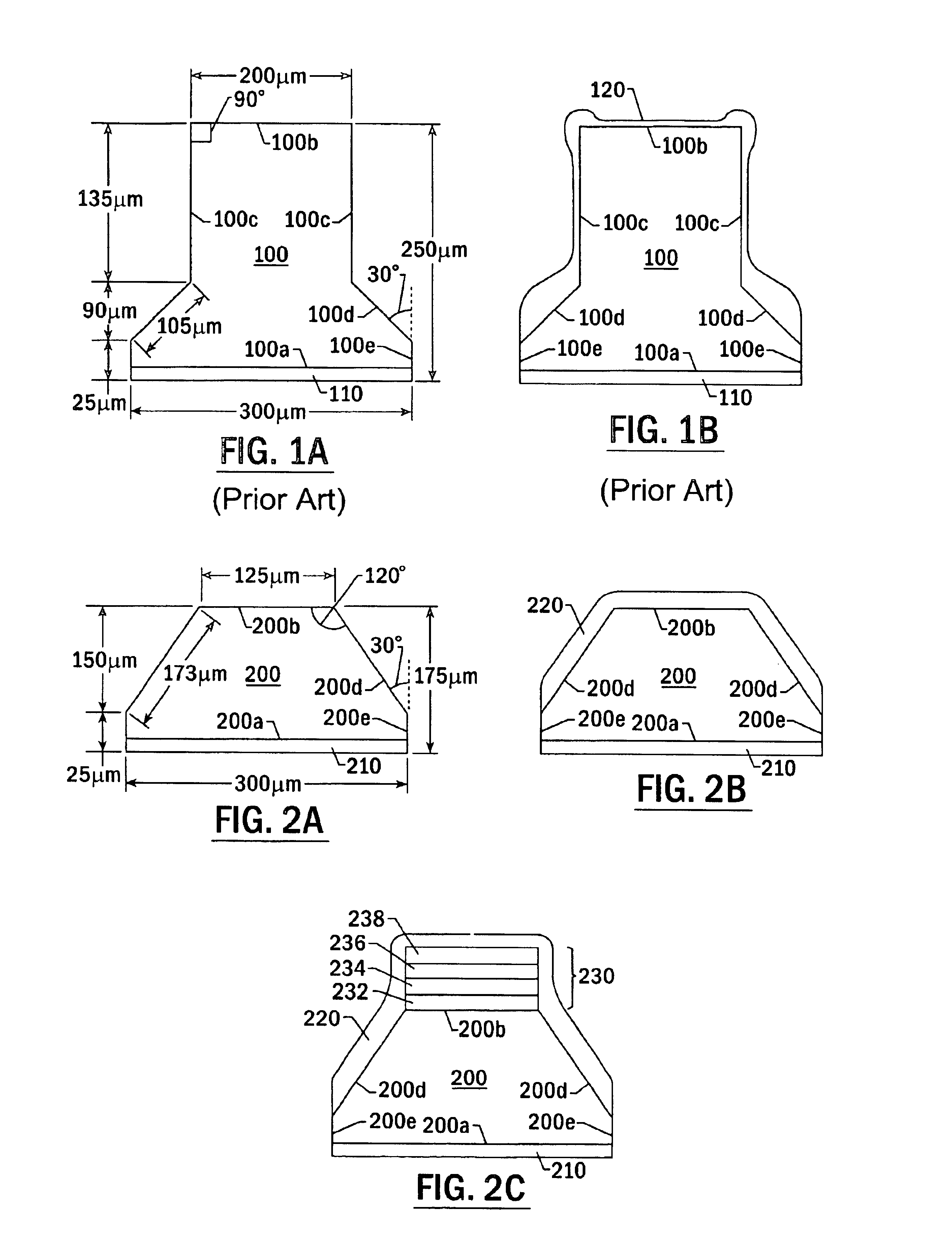
The present invention now will be described more fully hereinafter with reference to the accompanying drawings, in which embodiments of the invention are shown. However, this invention should not be construed as limited to the embodiments set forth herein. Rather, these embodiments are provided so that this disclosure will be thorough and complete, and will fully convey the scope of the invention to those skilled in the art. In the drawings, the thickness of layers and regions are exaggerated for clarity. Like numbers refer to like elements throughout. It will be understood that when an element such as a layer, region or substrate is referred to as being “on” or extending “onto” another element, it can be directly on or extend directly onto the other element or intervening elements may also be present. In contrast, when an element is referred to as being “directly on” or extending “directly onto” another element, there are no intervening elements present.

Embodiments of the invention...


PUM


Abstract

A light emitting diode includes a substrate having first and second opposing faces and a sidewall between the first and second opposing faces that extends at an oblique angle from the second face towards the first face. A conformal phosphor layer is provided on the oblique sidewall. The oblique sidewall can allow more uniform phosphor coatings than conventional orthogonal sidewalls.

Description

FIELD OF THE INVENTIONThis invention relates to microelectronic devices and fabrication methods therefor, and more particularly to light emitting diodes (LEDs) and fabrication methods therefor.BACKGROUND OF THE INVENTIONLight emitting diodes are widely used in consumer and commercial applications. As is well known to those having skill in the art, a light emitting diode generally includes a diode region on a microelectronic substrate. The microelectronic substrate may comprise, for example, silicon, gallium arsenide, gallium phosphide, alloys thereof, silicon carbide and / or sapphire. Continued developments in LEDs have resulted in highly efficient and mechanically robust light sources that can cover the visible spectrum and beyond. These attributes, coupled with the potentially long service life of solid state devices, may enable a variety of new display applications, and may place LEDs in a position to compete with the well entrenched incandescent and fluorescent lamps.One measure ...

Claims


Application Information

Patent Timeline
Patent Type & Authority Patents(United States)
IPC IPC(8): H01L33/00H01L33/20H01L33/50
CPCH01L33/505H01L33/20H01L33/24
Inventor SLATER, JR., DAVID B.NEGLEY, GERALD H.
Owner CREELED INC
Why Eureka
Try Eureka