
Heatsinking and packaging of integrated circuit chips

Inactive Publication Date: 2005-02-08
VOLTERRA SEMICONDUCTOR
View PDF10 Cites 59 Cited by
  • Summary
  • Abstract
  • Description
  • Claims
  • Application Information

AI Technical Summary

Benefits of technology

Implementations of the invention may include one or more of the following features. The rigid structure and the compressible material may be thermally conductive and / or electrically insulating. The semiconductor die may be a flipchip. The rigid structure may include a body having a groove formed therein, and the die may be located in the groove. A depth of the groove may be preselected to compress the compressible material by between about three-quarters and one-half. The compressible material may have an uncompressed depth of about 20 mils. The compressible material may be located between a top surface of the semiconductor die and a bottom surface of the groove. The compressible material may be sufficiently soft that it applies about 100 psi or less to the semiconductor die during attachment of the rigid structure to the printed circuit board. The compressible material may be a pad or a flowable material. The rigid structure may thermally contact the printed circuit board. A thermally conductive layer may be secured between the rigid structure and the printed circuit board. Mechanical fasteners, such as rivets, may secure the printed circuit board to the rigid structure.
Implementation of the invention may include one or more of the following features. A thermally conductive first layer may be located between the printed circuit board and the heatsink, and a thermally conductive second layer may be located between the semiconductor die and the heatsink. The first and second layers may be electrically insulating. The heatsink may include a bottom surface with a recess formed therein. A portion of the bottom surface surrounding the recess may provide the first surface, and a portion of the bottom surface in the recess may provides the second surface. Mechanical fasteners, such as rivets, may secure the heatsink to the printed circuit board. The die need not be secured to the heatsink. The first and second surfaces may be substantially flat.

Problems solved by technology

Due to significant power dissipation in integrated circuit (IC) chips, such as chip scale package (CSP) power devices, it is often necessary to attach an external heatsink in order to keep the device junction temperature below its rated value.
However, in CSP devices, the bare die is exposed to the environment.

Method used


Image

  • Heatsinking and packaging of integrated circuit chips
  • Heatsinking and packaging of integrated circuit chips

Examples


Embodiment Construction

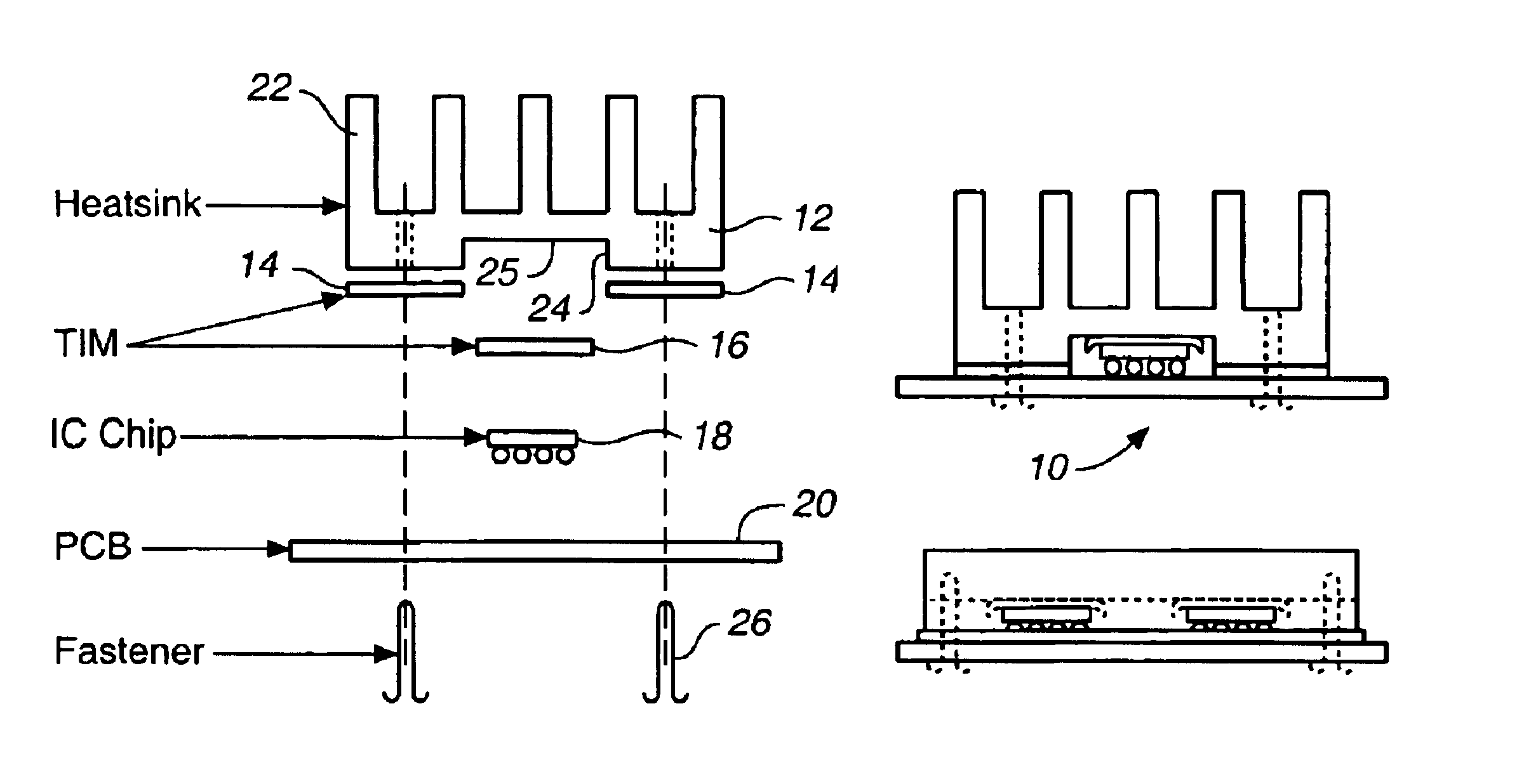
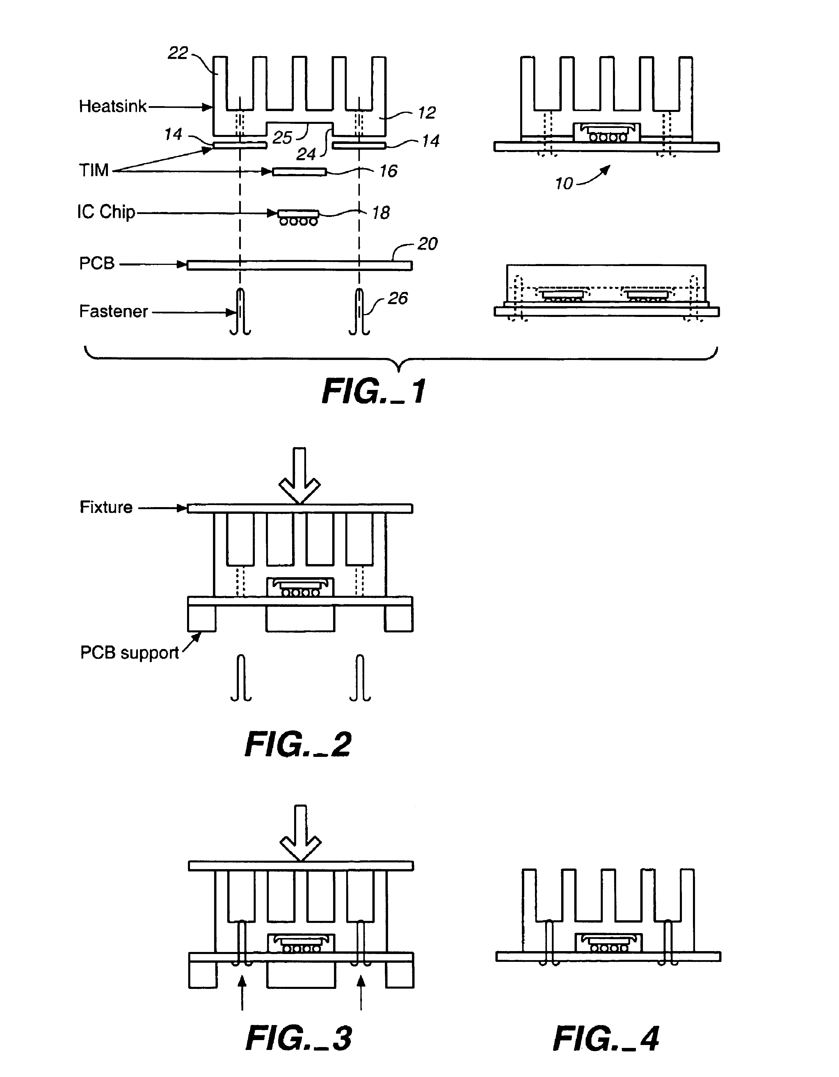
Referring to FIG. 1, a proposed semiconductor die package or heatsink assembly 10 includes a heatsink 12, the IC chip 18, a printed circuit board (PCB) 20, a first layer of thermally conductive electrically insulating interface material 16 between the IC chip 18 and the heatsink 12, an optional second layer of thermally conductive electrically insulating interface material 14 between the heatsink 12 and the printed circuit board 20, and one or more fasteners 26. The IC chip can be a chip scale package (CSP) power device with an exposed semiconductor die surface, and can be a flip-chip device. Optionally, the IC chip 18 can include an interface layer between the die and the printed circuit board 20.

The thermally conductive interface material 16 provides a first conductive thermal path from the heat generating device (CSP device 8) into the heatsink 12. In addition, the interface material 16 is soft, compliant and compressible to provide cushioning between the chip 18 and the heatsink...


PUM


Abstract

A semiconductor package has a printed circuit board, an integrated circuit chip on the printed circuit board with an exposed semiconductor die, and a rigid structure secured to the printed circuit board and enclosing the exposed semiconductor die. The exposed surface of the semiconductor die placed is in thermal contact with an inner surface of the rigid structure with a compressible material.

Description

BACKGROUNDThis invention relates to heatsinks and packaging of integrated circuit chips.Due to significant power dissipation in integrated circuit (IC) chips, such as chip scale package (CSP) power devices, it is often necessary to attach an external heatsink in order to keep the device junction temperature below its rated value. However, in CSP devices, the bare die is exposed to the environment. Therefore, special care must be taken to avoid excessive pressure when a heatsink is attached, in order to avoid damaging the die.Descriptions of various prior art heatsink packages can be found in the following patents: U.S. Pat. No. 5,367,193, entitled “Low cost, thermally efficient, and surface mountable semiconductor package for a high applied power VLSI die”, U.S. Pat No. 5,789,810, entitled “Semiconductor cap”, U.S. Pat. No. 5,905,636, entitled “Heat dissipation apparatus and method for attaching a heat dissipation apparatus to an electronic device”, U.S. Pat. No. 5,909,057, entitled...

Claims


Application Information

Patent Timeline
IPC IPC(8): H01L23/42H01L23/34H01L23/40H01L23/48
CPCH01L23/4093H01L23/42H01L24/72H01L2924/01006H01L2924/01029H01L2924/14H01L2224/16227H01L2224/73253
Inventor DJEKIC, OGNJEN
Owner VOLTERRA SEMICONDUCTOR
Learn More