

Circuit apparatus operable under high voltage
a high-voltage, circuit-based technology, applied in the direction of logic circuit coupling/interface arrangement, pulse technique, instruments, etc., can solve the problems of low operation voltage of the chip, difficult to design an analog circuit that may have a high operation voltage,
- Summary
- Abstract
- Description
- Claims
- Application Information
AI Technical Summary
Benefits of technology
Problems solved by technology
Method used
Image

Examples
first embodiment
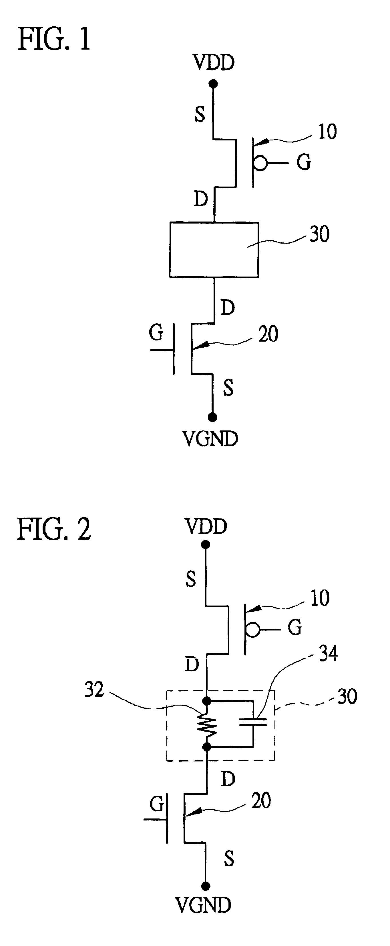
FIG. 2 shows a schematic illustration of the invention. Referring to FIG. 2, the circuit apparatus of this embodiment includes a PMOS transistor 10, an NMOS transistor 20, and an interface unit 30. The interface unit 30 includes a resistor 32 and a capacitor 34 connected to the resistor 32 in parallel. The resistor 32 may share a portion of the voltage difference (VDD-VGND) to define the voltage differences across the PMOS transistor 10 and the NMOS transistor 20, which are low-voltage devices, within the resistant range for the low-voltage devices. That is, the voltage differences across the PMOS transistor 10 and the NMOS transistor 20 are lower than the breakdown voltages of the PMOS transistor 10 and the NMOS transistor 20, respectively. Consequently, the PMOS transistor 10 and the NMOS transistor 20 are free from being burn out. In an analog circuit apparatus that operates normally, the current magnitude of the circuit apparatus is almost determined when the design is made. If ...
second embodiment
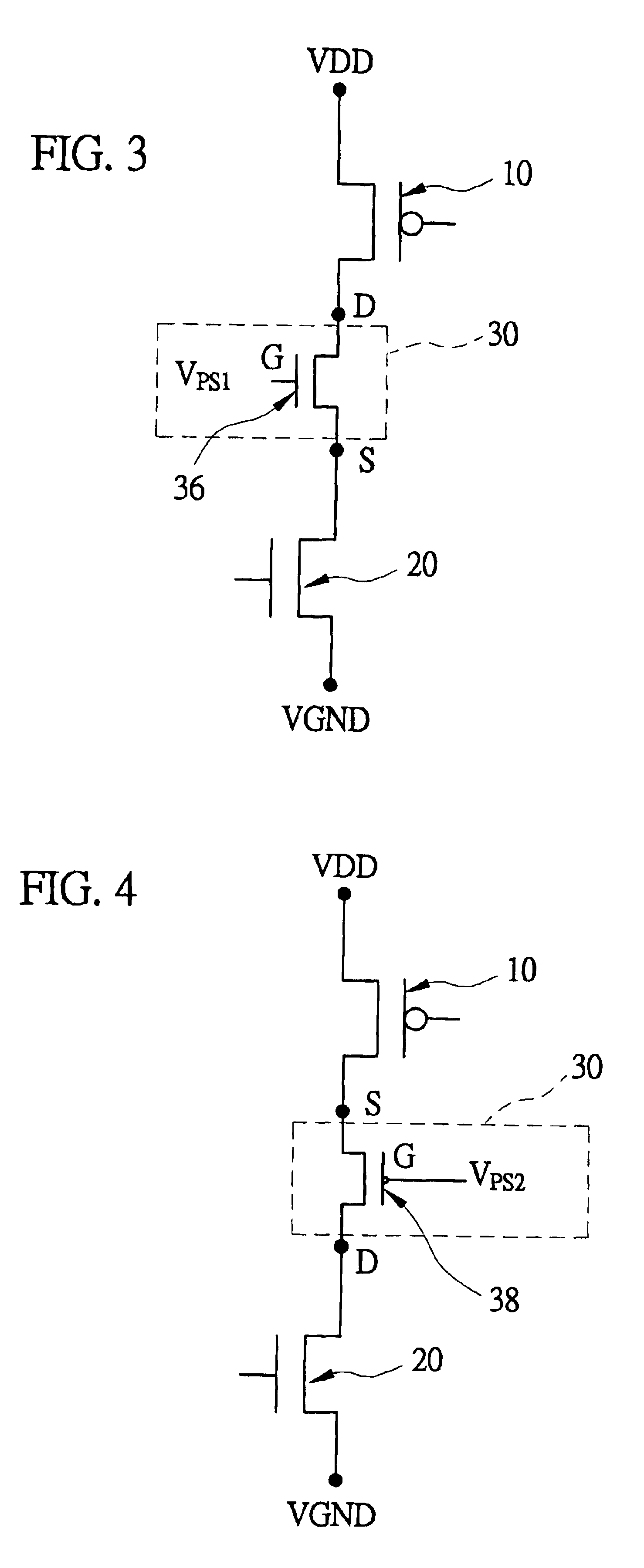
FIG. 3 shows a schematic illustration of the invention. Referring to FIG. 3, the interface unit 30 of this embodiment includes a high-voltage-resistant NMOS transistor 36 having a high operation voltage greater than the low operation voltage, and usually having a third breakdown voltage higher than the first breakdown voltage. Under some design considerations, the NMOS transistor 36 may also has a third breakdown voltage equal to or smaller than the first breakdown voltage. The gate G of the NMOS transistor 36 is coupled to a first control signal VPS1 of the power-saving mode, and the first control signal VPS1, is a low-voltage signal when the circuit apparatus is in the power-saving mode.
The NMOS transistor 36 may operate in the triode region and the saturation region.
When the NMOS transistor 36 operates in the triode region, it may be regarded as a resistor having a resistance R that may be expressed in the following equation: R≈1μ0COX(VGS-Vτ),(1)wherein μ0 denotes the electron ...
third embodiment
FIG. 4 shows a schematic illustration of the invention. Referring to FIG. 4, the interface unit 30 of this embodiment includes a high-voltage-resistant PMOS transistor 38 having a gate coupled to a second control signal VPS2 of the power-saving mode, and the second control signal VPS2 is a high-voltage signal when the circuit apparatus is in the power-saving mode.
The PMOS transistor 38 also may operate in the triode region and the saturation region.
When the PMOS transistor 38 operates in the triode region, it may be regarded as a resistor having a resistance that may be expressed by the same Equation (a) as that of the NMOS transistor 36.
Under the normal operation, the principle is the same as that of the second embodiment, and the function of the resistance is the same as that of the first embodiment.
When the PMOS transistor 38 operates in the saturation region, the low-voltage PMOS transistor 10 coupled to the source S of the PMOS transistor 38 may be regarded as a current source ...
PUM
 Abstract
Description
Claims
Application Information