Selective thermal transfer of light emitting polymer blends

a technology of light-emitting polymer and blend, which is applied in the direction of thermal imaging, natural mineral layered products, printing, etc., can solve the problems of difficult selective thermal transfer of high-fidelity leps, and difficult to achieve high-fidelity selective thermal transfer of leps. , the effect of improving thermal transfer fidelity

Inactive Publication Date: 2005-02-15
SAMSUNG DISPLAY CO LTD
View PDF26 Cites 71 Cited by
  • Summary
  • Abstract
  • Description
  • Claims
  • Application Information

AI Technical Summary

Benefits of technology

Selective thermal transfer of organic electroluminescent materials (also referred to as organic light emitters), and more specifically of light emitting polymers (LEPs), can be important in patterning organic light emitting devices (OLEDs, also referred to as organic electroluminescent devices). More traditional patterning methods including photolithographic techniques, shadow mask techniques, screen printing techniques, and others, have been problematic in patterning organic light emitters, especially for making OLEDs based on LEPs and / or in making high resolution pixilated displays. Selective thermal transfer can be a viable patterning method for a wide variety of organic light emitters and for a wide variety of display constructions.
Some LEPs can be difficult to selectively thermally transfer with high fidelity in their pure form. In many cases, this might be attributed to physical and mechanical properties of the film or coating of LEP material being transferred. Some physical and mechanical properties that may be important include molecular weight, intra-layer cohesive strength, and the like. The present invention contemplates blending LEPs with other materials to modify the physical and / or mechanical properties of the LEP-based emissive layer being patterned to improve thermal transfer fidelity while maintaining desired functionality of the emissive layer in an OLED.
In one embodiment, the present invention provides a thermal transfer donor element that includes a substrate and a transfer layer capable of being selectively thermally transferred from the donor element, the transfer layer including a blend of a light emitting polymer and an additive. The additive can be selected to promote high fidelity thermal transfer of the transfer layer. The blend is capable of forming the emissive layer of an organic electroluminescent device.
In another embodiment, the present invention provides a process for patterning a light emitting polymer, including the steps of providing a thermal transfer donor element, bringing the donor clement into close proximity with a receptor substrate, and selectively thermally transferring the transfer layer from the donor to the receptor. The donor element includes a substrate and a transfer layer that includes a blend of a light emitting polymer and an additive. The additive can be selected to promote high fidelity thermal transfer of the transfer layer. The blend is capable of forming the emissive layer of an organic electroluminescent device.

Problems solved by technology

More traditional patterning methods including photolithographic techniques, shadow mask techniques, screen printing techniques, and others, have been problematic in patterning organic light emitters, especially for making OLEDs based on LEPs and / or in making high resolution pixilated displays.
Some LEPs can be difficult to selectively thermally transfer with high fidelity in their pure form.

Method used


Image

  • Selective thermal transfer of light emitting polymer blends
  • Selective thermal transfer of light emitting polymer blends

Examples


example 1

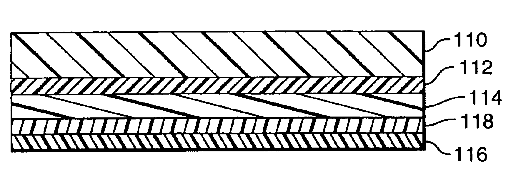
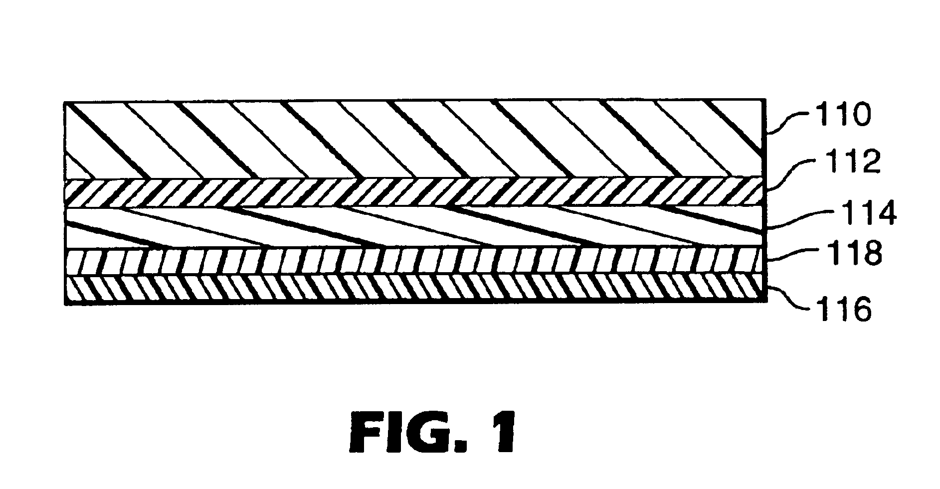
Preparation of a Receptor with a PEDT / PSS Buffer Layer

A receptor substrate having a PEDT / PSS buffer layer was prepared in the following manner.

An indium tin oxide (ITO) striped substrate was spin coated at 2000 r.p.m. with a buffer solution consisting of poly(3,4-ethylenedioxythiophene) / poly(styrene sulfonicacid) (PEDT / PSS) in de-ionized water (99.5:0.5 water to PEDT / PSS, by weight). The PEDT / PSS buffer material was the PEDT / PSS commercially available from Bayer Corporation under the trade designation Baytron P 4083. The PEDT / PSS coated substrate was heated at 110° C. on a hot plate for 5 minutes in air. The PEDT / PSS coating serves as a hole injecting buffer layer in OLEDs.

example 2

Preparation of a Receptor with an Active Primer Layer

A receptor substrate having an active primer layer was prepared in the following manner.

An indium tin oxide (ITO) striped substrate was spin coated at 2000 r.p.m. with a buffer solution consisting of PEDT / PSS in de-ionized water (70:30 water to PEDT / PSS, by weight). The PEDT / PSS coated substrate was heated at 110° C. on a hot plate for 5 minutes in air. The PEDT / PSS coating served as a hole injecting buffer layer in the patterned OLEDs (see Example 7). An active primer layer was then coated over the PEDT / PSS coating. The active primer layer was a 1:1 dispersion of bis(3-methylphenyl)N,N′ dimethylbenzidine (TPD) in polystyrene (50,000 MW, available from Polysciences). The TPD was obtained from Aldrich Chemical Company, Milwaukee, Wis. The polystyrene used had a 50,000 molecular weight and was obtained from Polysciences, Warrington, Pa. The active primer was spin coated onto the PEDT / PSS layer out of a 1.5% weight-to-volume toluene ...

example 4

Preparation of a Donor Sheet with a PPV / Polystyrene Blend Transfer Layer

A thermal transfer donor sheet having a light emitting polymer blend transfer layer was prepared in the following manner.

An LTHC solution was coated onto a 0.1 mm thick PET film substrate as in Example 3. Next, an interlayer was coated onto the cured LTHC layer as in Example 3. Next, a 1:1 by weight blend of a PPV light emitting polymer and polystyrene was spin coated out of a 0.5% weight-to-volume toluene solution onto the cured interlayer. The PPV was one commercially available from Covion Organic Semiconductors GmbH, Frankfurt, Germany, and identified as COVION PDY 132. The polystyrene used had a 50,000 molecular weight and was obtained from Polysciences, Warrington, Pa.


PUM

PropertyMeasurementUnit
thickaaaaaaaaaa
thickaaaaaaaaaa
thicknessaaaaaaaaaa

Abstract

The present invention provides a selectively thermally transferable blend capable of forming the emissive layer of an organic electroluminescent device. The blend includes a light emitting polymer and an additive selected to promote selective thermal transfer of the blend from a donor element to a proximately located receptor substrate.

Description

BACKGROUNDPattern-wise thermal transfer of materials from donor sheets to receptor substrates has been proposed for a wide variety of applications. For example, materials can be selectively thermally transferred to form elements useful in electronic displays and other devices. Specifically, selective thermal transfer of color filters, black matrix, spacers, polarizers, conductive layers, transistors, phosphors, and organic electroluminescent materials have all been proposed. Selective thermal transfer of organic light emitters for formation of organic electroluminescent devices has been shown to be particularly useful.SUMMARY OF THE INVENTIONSelective thermal transfer of organic electroluminescent materials (also referred to as organic light emitters), and more specifically of light emitting polymers (LEPs), can be important in patterning organic light emitting devices (OLEDs, also referred to as organic electroluminescent devices). More traditional patterning methods including phot...

Claims


Application Information

Patent Timeline
Patent Type & Authority Patents(United States)
IPC IPC(8): H01L51/40H01L51/05H01L51/30H05B33/10B41M3/06B41M5/382B41M5/385B41M5/395H01L51/00H01L51/50
CPCB41M5/38207H01L51/0013B41M5/38214H01L51/0059H01L51/0037H01L51/0038H10K71/18H10K85/114H10K85/1135H10K85/631B41M5/382B41M5/035
Inventor NIRMAL, MANOJLE, HA T.WOLK, MARTIN B.BELLMANN, ERIKAMCCORMICK, FRED
Owner SAMSUNG DISPLAY CO LTD
Why Eureka
Try Eureka