Semiconductor nano-rod devices

a technology of semiconductor devices and nanorods, which is applied in the direction of semiconductor devices, electrical equipment, nanotechnology, etc., can solve the problems of parasitic off-state leakage, gate oxide thickness, and difficult to meet body-doping concentration requirements, and achieve the effect of reducing the number of transistors

Inactive Publication Date: 2005-02-15
TAIWAN SEMICON MFG CO LTD
View PDF9 Cites 182 Cited by
  • Summary
  • Abstract
  • Description
  • Claims
  • Application Information

AI Technical Summary

Benefits of technology

For a more complete understanding of the present invention, and the advantages thereof, reference is now made to the following descriptions taken in conjunction with the accompanying drawings, in which:
FIGS. 1A, 2A, 3A, 4A, 5A, and 6A show simplified perspective views of one transistor device being m...

Problems solved by technology

Hence, a transistor with a short gate length often suffers from problems related to the inability of the gate to substantially control the on/off states of the channel, which is often called short-channel effects.
However, for device scaling well into the sub-30 nm regime, the requirements for body-doping concentration, gate oxide thickness, and source/drain doping...

Method used


Image

  • Semiconductor nano-rod devices
  • Semiconductor nano-rod devices
  • Semiconductor nano-rod devices

Examples


Embodiment Construction

The use of presently preferred embodiments are discussed in detail below. It should be appreciated, however, that the present invention provides many applicable inventive concepts that can be embodied in a wide variety of specific contexts. The specific embodiments discussed are merely illustrative of specific ways to make and use the invention, and do not limit the scope of the invention.

Example embodiments of the present invention will be described herein in a specific context of making semiconductor devices, such as transistors. In other embodiments not shown, embodiments of the present invention also may include nano-wires or quantum-wires formed in accordance with the present invention. The present invention may also be applied, however, to other situations.

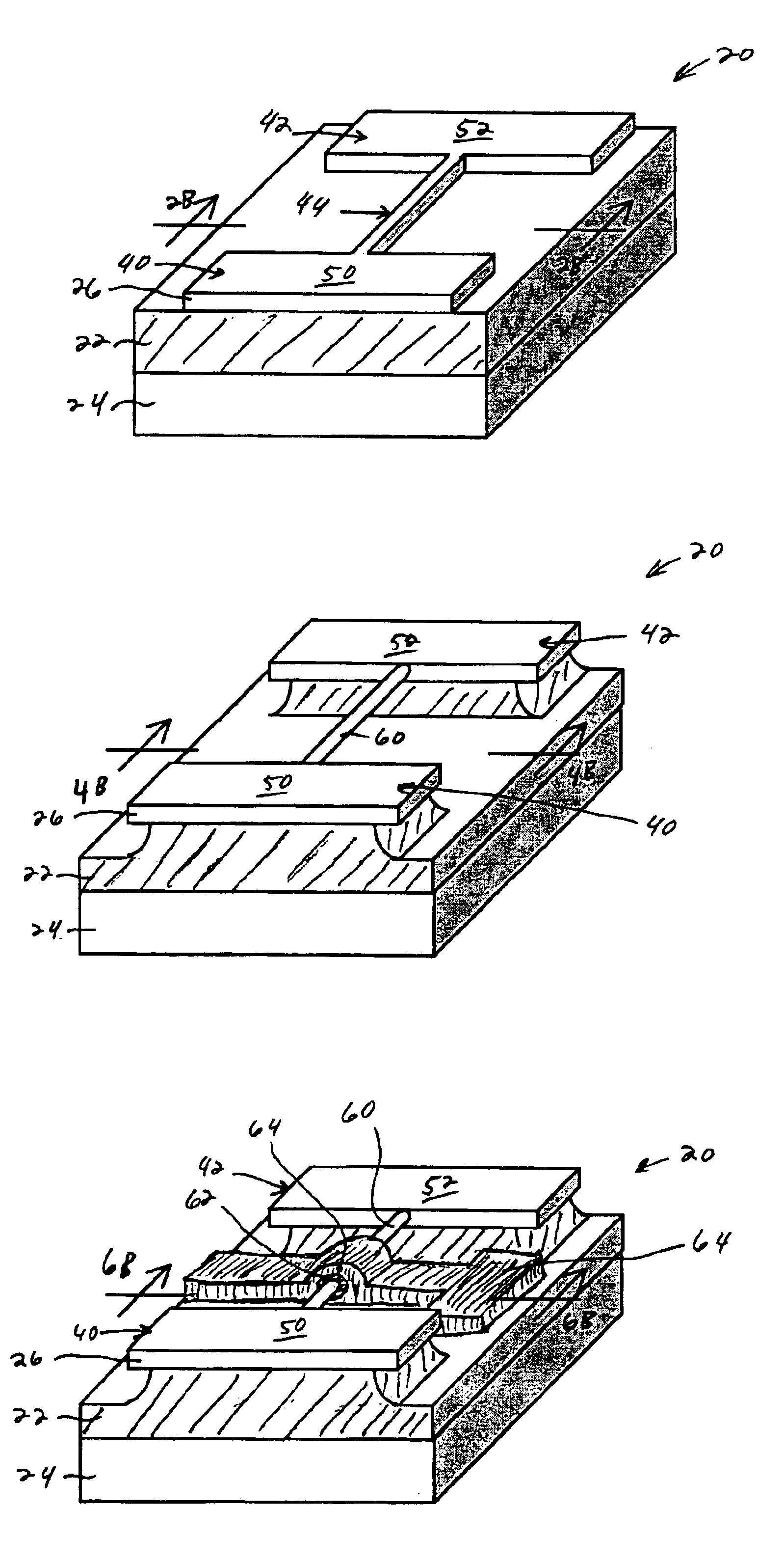
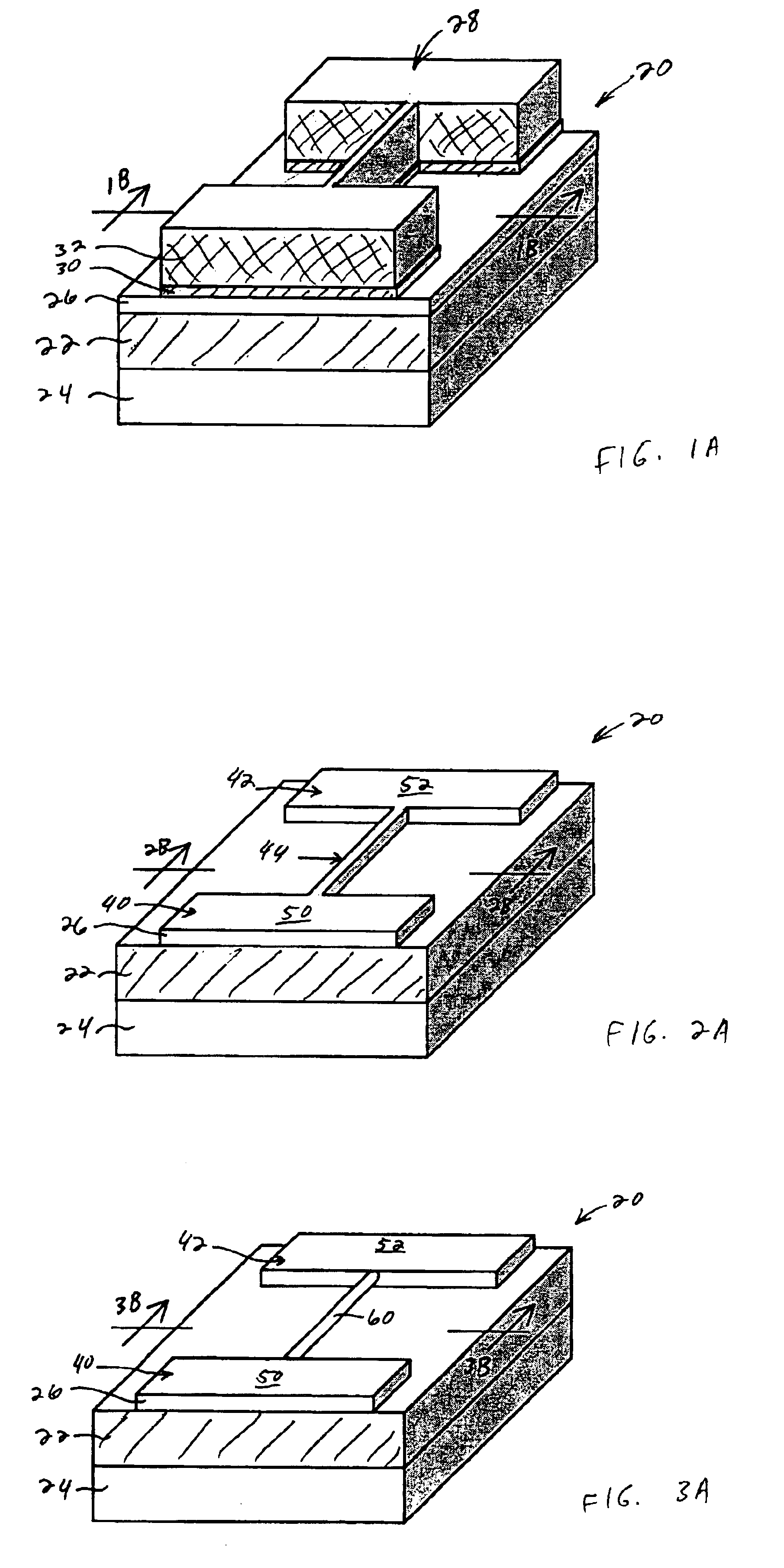
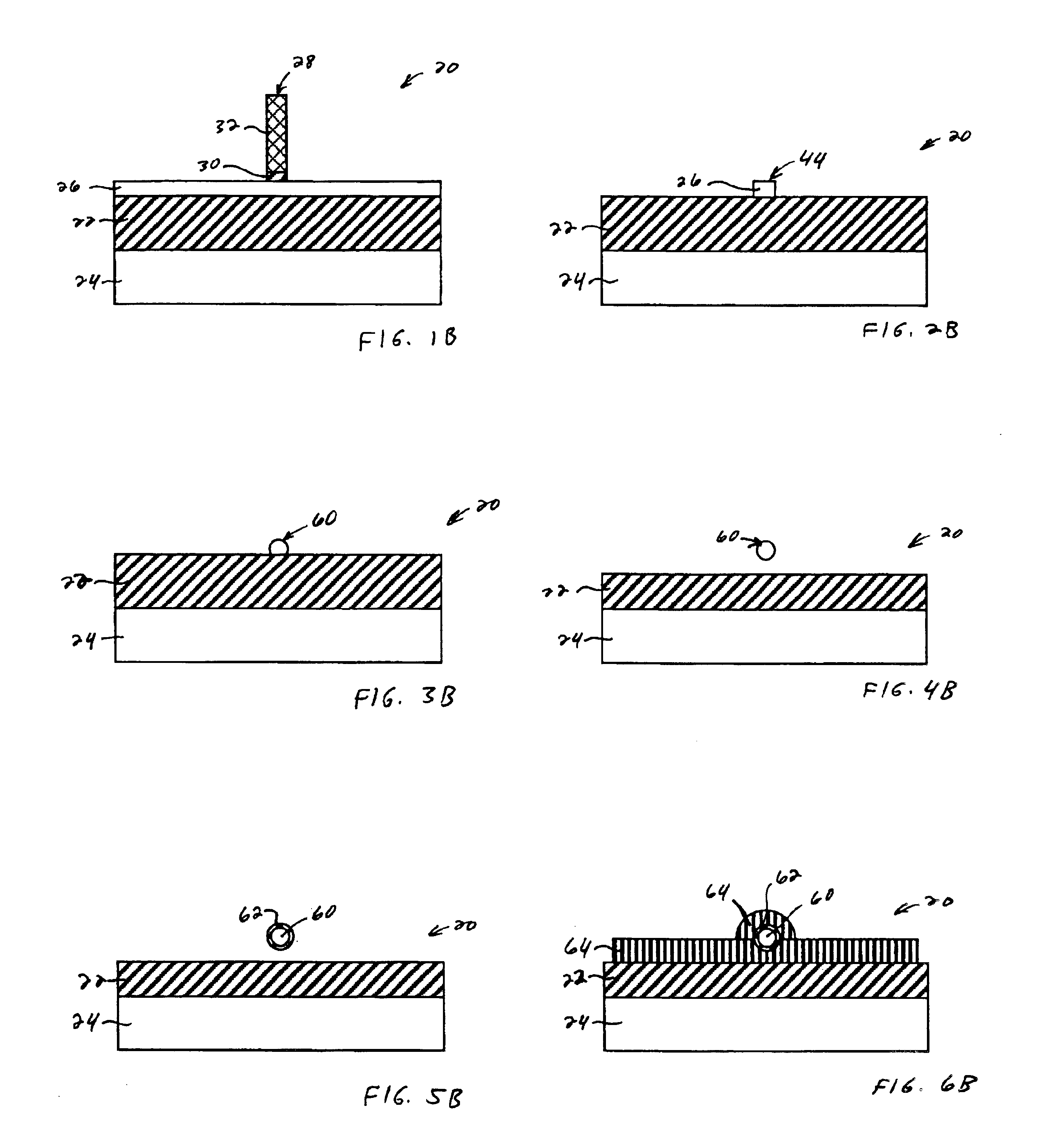
A preferred manufacturing process in accordance with the present invention may be used to make a transistor device. Some of the manufacturing steps of this preferred embodiment being used to make a transistor embodiment are ...


PUM


Abstract

In a method of manufacturing a semiconductor device, a semiconductor layer is patterned to form a source region, a channel region, and a drain region in the semiconductor layer. The channel region extends between the source region and the drain region. Corners of the channel region are rounded by annealing the channel region to form a nano-rod structure. Part of the nano-rod structure is then used as a gate channel. Preferably, a gate dielectric and a gate electrode both wrap around the nano-rod structure, with the gate dielectric being between the nano-rod structure and the gate electrode, to form a transistor device.

Description

TECHNICAL FIELDThe present invention relates generally to methods for manufacturing semiconductor devices. In one aspect, the present invention relates to a method of forming a nano-rod structure for a channel of a field effect transistor.BACKGROUNDMetal-oxide-semiconductor field effect transistor (MOSFET) technology is currently the dominant semiconductor technology used for manufacturing ultra-large scale integrated (ULSI) circuits. As the gate length of the MOSFET is scaled down into the sub-30 nm regime for improved performance and density, the source and drain increasingly interact with the channel to sometimes gain influence on the channel potential. Hence, a transistor with a short gate length often suffers from problems related to the inability of the gate to substantially control the on / off states of the channel, which is often called short-channel effects.Increased body doping concentration, reduced gate oxide thickness, and junction depths are some ways to suppress short-...

Claims


Application Information

Patent Timeline
IPC IPC(8): H01L21/02H01L29/786H01L29/66H01L21/336H01L29/423H01L29/40H01L29/775
CPCB82Y10/00H01L29/0673H01L29/42384H01L29/7854H01L29/66742H01L29/66795H01L29/42392H01L29/775
Inventor CHEN, HAO-YUYEO, YEE-CHIAYANG, FU-LIANGHU, CHENMING
Owner TAIWAN SEMICON MFG CO LTD
Why Eureka
Try Eureka