Method of manufacture of programmable switching circuits and memory cells employing a glass layer

Inactive Publication Date: 2005-02-22
MICRON TECH INC
View PDF227 Cites 98 Cited by
  • Summary
  • Abstract
  • Description
  • Claims
  • Application Information

AI Technical Summary

Benefits of technology

In a preferred embodiment, a liner layer of an insulating material that conforms to the cells and the semiconductor base material is deposited over the cells. This liner layer acts as a barrier to prevent diffusion of the metal away from

Problems solved by technology

Electric power must be supplied to the capacitors to maintain the information because, without frequent refresh cycles, the stored charge dissipates, and the information is lost.
H

Method used


Image

  • Method of manufacture of programmable switching circuits and memory cells employing a glass layer
  • Method of manufacture of programmable switching circuits and memory cells employing a glass layer
  • Method of manufacture of programmable switching circuits and memory cells employing a glass layer

Examples


Embodiment Construction

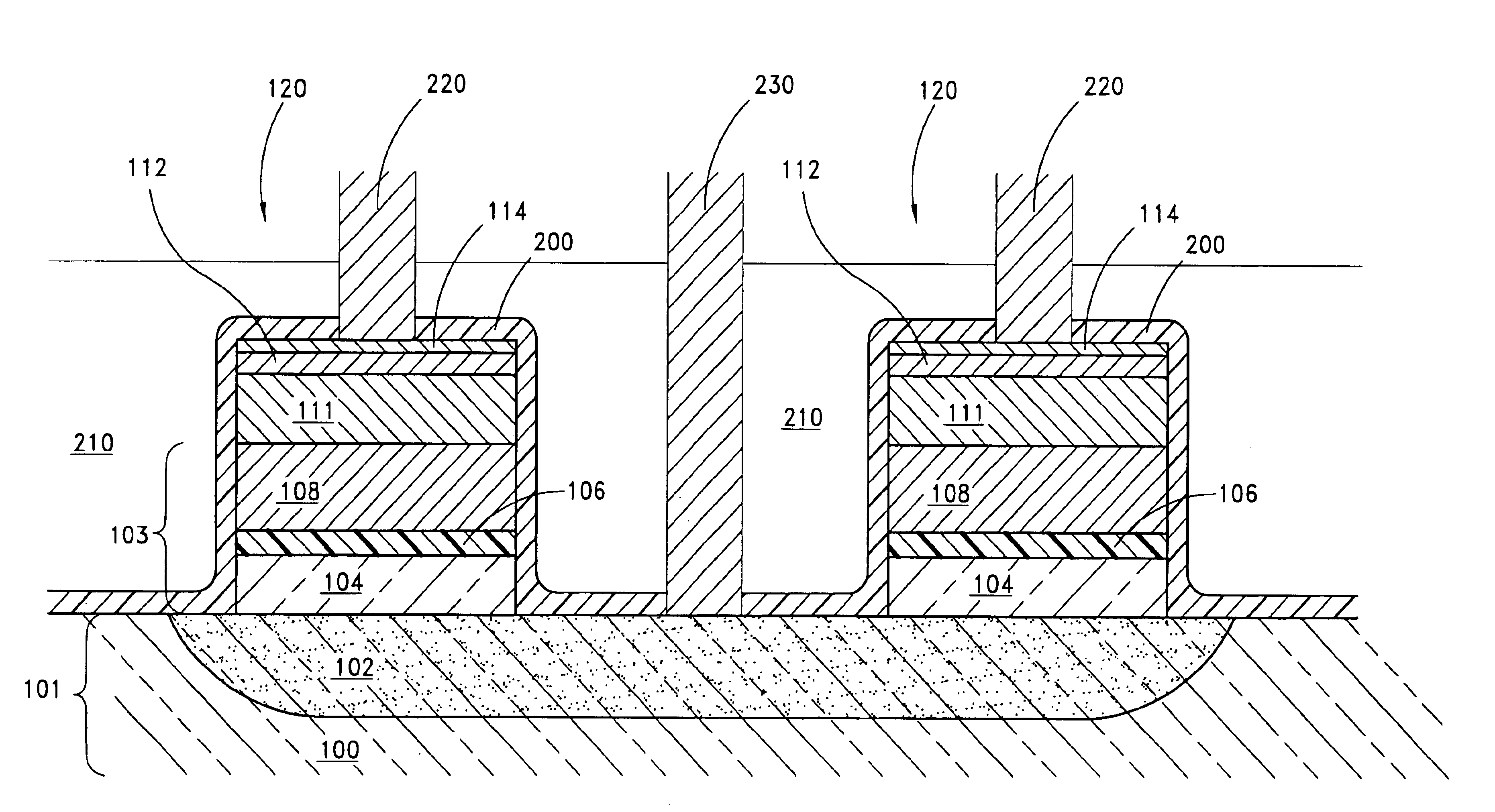
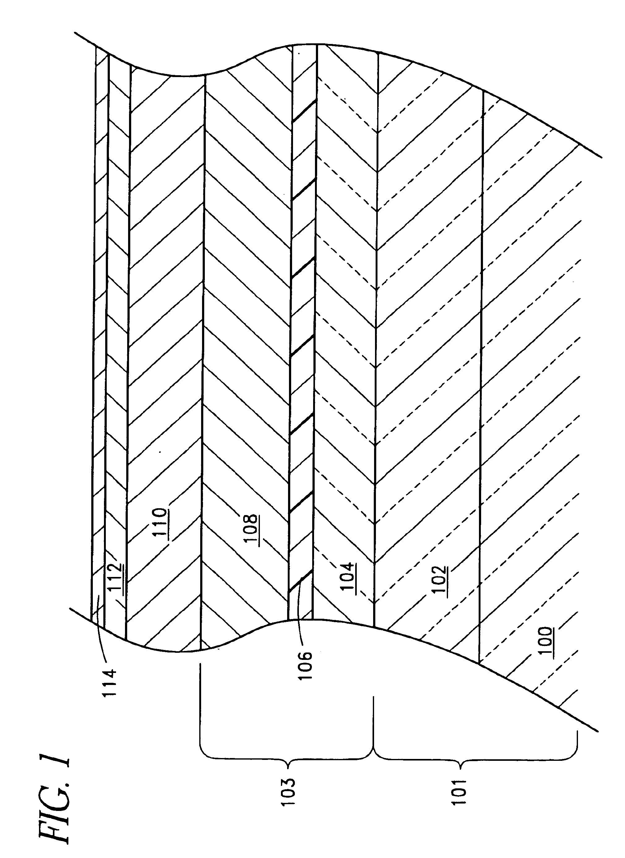
The preferred embodiment discloses a method of fabricating a programmable memory cell in a stud configuration. Blanket layers of electrode and body materials are deposited and subsequently patterned and etched, leaving pillars or studs as individual devices. The blanket deposition of the layers avoids problems associated with via filling and allows more flexibility in cell configuration.

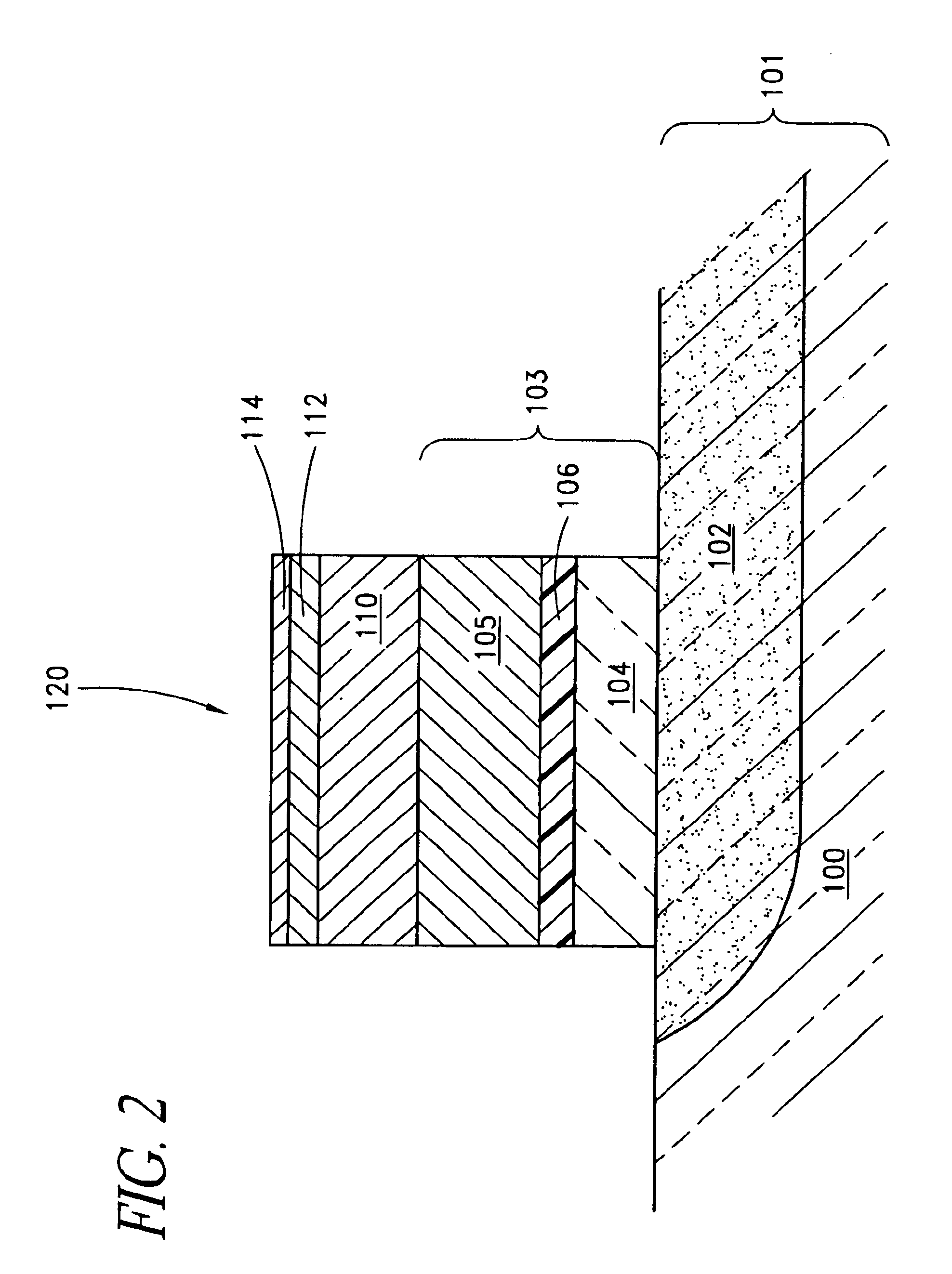
With reference to FIG. 1, a cross section of deposited blanket layers is shown. A semiconductor base material 100 containing a heavily doped (e.g., n+) conductive region 102 comprises the substrate 101 upon which the memory cells are fabricated. In general, the substrate comprises the lowest layer of semiconductor material from which devices are formed in the integrated circuit. In the illustrated embodiments, the substrate comprises a single-crystal silicon wafer. In other arrangements, an epitaxial silicon layer or another semiconductor, such as a III-V material, can be used.

A bottom electrode 103 ...


PUM

PropertyMeasurementUnit
Widthaaaaaaaaaa
Widthaaaaaaaaaa
Wavelengthaaaaaaaaaa

Abstract

Programmable conductor memory cells in a stud configuration are fabricated in an integrated circuit by blanket deposition of layers. The layers include a bottom electrode in contact with a conductive region in a semiconductor substrate, a glass electrolyte layer that forms the body of the cell and a top electrode layer. Under the influence of an applied voltage, conductive paths grow through or along the cell body. The layers are patterned and etched to define separate pillars or cells of these stacked materials. A liner layer of an insulating material is deposited over the cells and acts as a barrier to prevent diffusion of the metal in the cell body into other parts of the integrated circuit. Remaining regions between the cells are filled with an insulating layer. At least some of the insulating layer and some of the liner layer are removed to make contact to the top electrode layer of the cell and to the substrate.

Description

BACKGROUND OF THE INVENTION1. Field of the InventionThis invention relates generally to a method of manufacture of memory devices for integrated circuits and more particularly to programmable conductor memory arrays comprising glass electrolyte elements.2. Description of the Related ArtThe digital memory most commonly used in computers and computer system components is the dynamic random access memory (DRAM), wherein voltage stored in capacitors represents digital bits of information. Electric power must be supplied to the capacitors to maintain the information because, without frequent refresh cycles, the stored charge dissipates, and the information is lost. Memories that require constant power are known as volatile memories.Non-volatile memories do not need frequent refresh cycles to preserve their stored information, so they consume less power than volatile memories. The information stays in the memory even when the power is turned off. There are many applications where non-vola...

Claims


Application Information

Patent Timeline
IPC IPC(8): B32B9/04H01L21/02H01L21/44H01L21/302H01L21/461G11C16/02H01L21/8242H01L27/24H01L45/00
CPCG11C13/0011H01L27/2463H01L45/085H01L45/143H01L45/1658H01L45/1675H01L45/1233Y10T428/24917H10B63/80H10N70/245H10N70/8825H10N70/046H10N70/063H10N70/826
Inventor GILTON, TERRY L.
Owner MICRON TECH INC
Why Eureka
Try Eureka