Evaluation method for evaluating insulating film, evaluation device therefor and method for manufacturing evaluation device

a technology of insulating film and evaluation device, which is applied in the direction of individual semiconductor device testing, semiconductor/solid-state device testing/measurement, instruments, etc., can solve the problems of gate oxide film punching, inability to observe, and inability to reliably evaluate damage, so as to achieve easy and reliable evaluation

Inactive Publication Date: 2005-02-22
PANASONIC CORP
View PDF4 Cites 4 Cited by
  • Summary
  • Abstract
  • Description
  • Claims
  • Application Information

AI Technical Summary

Benefits of technology

The present invention has been made to solve these problems in the prior art and has an object to make it possible to easily and reliably evaluate damage to an insulating film occurring in the dry etching step across the entire surface of a semiconductor substrate.
With the method for evaluating an insulating film of the present invention, it is possible to electrically observe the condition of an insulating film on a semiconductor substrate without using an optical method such as a microscope. As a result, it is possible to easily and reliably evaluate a damage to the insulating film occurring in the dry etching step across the entire surface of the semiconductor substrate.
In this way, the etchant of the dry etching is localized in a region of the insulating film that is surrounded by the teeth, i.e., protruding portions, of the comb-shaped electrode pattern, thereby increasing the damage to the insulating film. Thus, it is possible to increase the leakage current measurement sensitivity.
As described above, the device for evaluating an insulating film of the present invention includes: the first insulating film formed on the upper surface of the semiconductor substrate including the p-n junction therein; the electrode pattern selectively formed on the first insulating film; and the measurement electrode formed on the first insulating film, with the second insulating film being interposed between the electrode pattern and the measurement electrode, whereby it is possible to reliably realize the method for evaluating an insulating film of the present invention.
According to the method for manufacturing an insulating film evaluation device of the present invention, the first insulating film is formed on the upper surface of the semiconductor substrate including the first semiconductor region of the first conductivity type formed in the upper portion of the semiconductor substrate, and the electrode pattern is selectively formed on the first insulating film. Then, the impurity of the second conductivity type is introduced into the semiconductor substrate using the electrode pattern as a mask so as to form the second semiconductor region of the second conductivity type in the upper portion of the first semiconductor region, thereby forming the p-n junction at the interface between the first semiconductor region and the second semiconductor region. Furthermore, the measurement electrode is formed on the first insulating film, with the second insulating film being interposed between the electrode pattern and the measurement electrode. Thus, it is possible to reliably obtain the insulating film evaluation device of the present invention.

Problems solved by technology

Accordingly, how to suppress the damage to the gate insulating film due to the dry etching step of forming a gate electrode by patterning has been an important problem in the art.
However, the conventional method for forming a gate electrode has a problem in that a punch-through occurs in the gate oxide film 102 when the thickness of the gate oxide film 102 is reduced to be 10 nm or less.
However, the conventional method for evaluating a gate oxide film has a problem in that it is not possible to evaluate and observe the entire surface of the semiconductor substrate 101, and another problem in that visual observation is instable and unreliable.

Method used


Image

  • Evaluation method for evaluating insulating film, evaluation device therefor and method for manufacturing evaluation device
  • Evaluation method for evaluating insulating film, evaluation device therefor and method for manufacturing evaluation device
  • Evaluation method for evaluating insulating film, evaluation device therefor and method for manufacturing evaluation device

Examples


first embodiment

The first embodiment of the present invention will now be described with reference to the drawings.

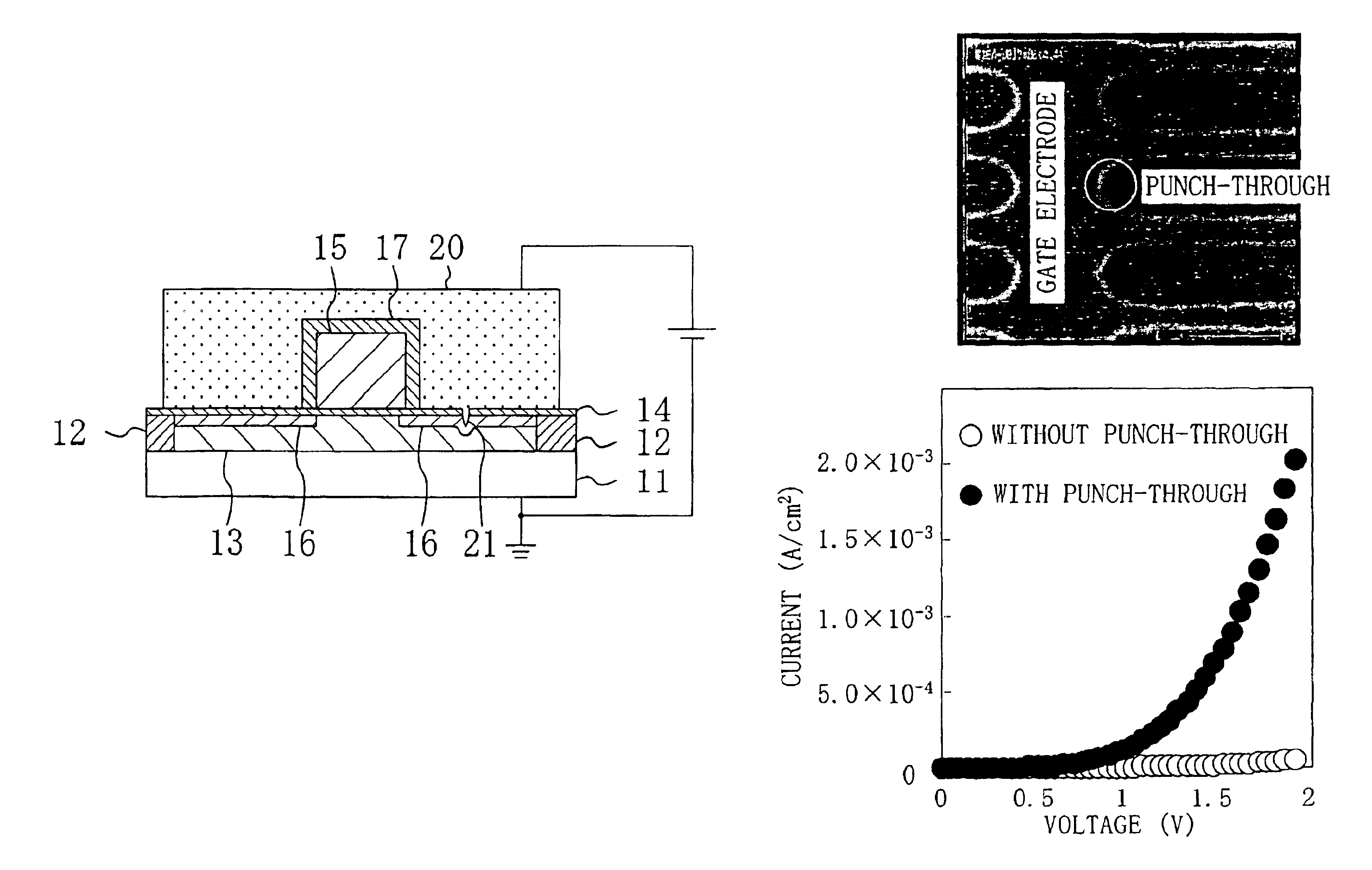
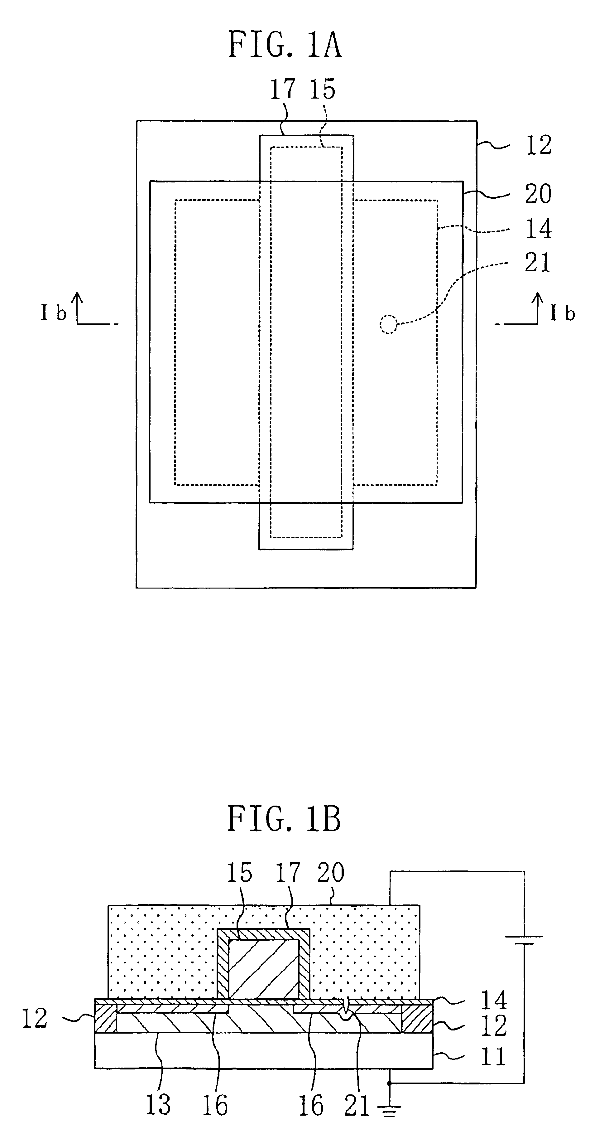
FIG. 1A and FIG. 1B illustrate a device for evaluating a gate insulating film according to the first embodiment of the present invention, wherein FIG. 1A is a plan view, and FIG. 1B is a cross-sectional view taken along line Ib—Ib of FIG. 1A. Herein, a device for evaluating the presence / absence of a damage to a gate insulating film on an active region of one of a plurality of transistors formed on a semiconductor wafer is illustrated for ease of understanding.

As illustrated in FIG. 1A and FIG. 1B, a semiconductor substrate (wafer) 11 made of silicon (Si), for example, includes, in an upper portion thereof, device isolation regions 12 made of silicon oxide (SiO2) and a p+-type layer 13 surrounded by the device isolation regions 12.

A gate insulating film 14 is formed by a thermal oxidization method, for example, on the principal surface of the semiconductor substrate 11, and a gate elect...

second embodiment

The second embodiment of the present invention will now be described with reference to the drawings.

FIG. 5A to FIG. 5E are cross-sectional views sequentially illustrating steps of a method for manufacturing a device for evaluating a gate insulating film according to the second embodiment of the present invention.

First, as illustrated in FIG. 5A, the device isolation regions 12 having a shallow trench structure, for example, are selectively formed in an upper portion of the semiconductor substrate 11 made of silicon. Then, a p-type impurity ion such as boron (B) ion is implanted into the semiconductor substrate 11 so as to form a p+-type layer 13 to be a p-type well.

Then, as illustrated in FIG. 5B, the gate insulating film 14 having a thickness of about 2 nm, for example, is deposited across the entire principal surface of the semiconductor substrate 11 by using a thermal oxidization method, or the like. Then, a gate electrode forming film made of polycrystalline silicon doped with a...

third embodiment

The third embodiment provides an improved detection sensitivity in detecting the presence / absence of a damage to a gate insulating film as compared with the device for evaluating a gate insulating film of the first or second embodiment. Again, a device for evaluating the presence / absence of a damage to a gate insulating film on an active region of one of a plurality of transistors formed on a semiconductor wafer is illustrated for ease of understanding. Note that in FIG. 6A, those elements that are already shown in FIG. 1A are denoted by the same reference numerals and will not be further described below.

As illustrated in FIG. 6A, a gate electrode 25 of the third embodiment includes protruding portions 25a that are protruding in a comb-like shape in the gate length direction from both sides of the gate electrode 25. Note that although not shown in the figure, the upper surface and the side surface of the gate electrode 25 are covered with an insulating film that electrically insulat...


PUM


Abstract

A method for evaluating an insulating film includes: a first step of forming an insulating film on a semiconductor substrate including a p-n junction therein; a second step of selectively forming an electrode pattern on the insulating film; a third step of forming a measurement electrode on the insulating film so as to be electrically insulated from the electrode pattern; and a fourth step of applying a measurement voltage between the measurement electrode and the semiconductor substrate via the insulating film and measuring a leakage current leaking through the p-n junction so as to evaluate a damage to the insulating film or the semiconductor substrate.

Description

BACKGROUND OF THE INVENTIONThe present invention relates to an evaluation method for evaluating the presence / absence of a damage to an insulating film, an evaluation device therefor, and a method for manufacturing the evaluation device.In recent years, along with the demand for increasing the speed and performance of LSIs, the thickness of a gate insulating film of a MIS transistor has been reduced. Accordingly, how to suppress the damage to the gate insulating film due to the dry etching step of forming a gate electrode by patterning has been an important problem in the art.A conventional method for forming a gate electrode made of polycrystalline silicon will now be outlined with reference to FIG. 11A and FIG. 11B.First, as illustrated in FIG. 11A, a gate oxide film 102 having a thickness of about 2 nm is formed on the principal surface of a semiconductor substrate 101 made of silicon, including a p-type well 101a formed in an upper portion thereof, and then a gate forming film 10...

Claims


Application Information

Patent Timeline
Patent Type & Authority Patents(United States)
IPC IPC(8): H01L21/66
CPCH01L22/14
Inventor YAMANAKA, MICHINARIYAMADA, TAKAYUKINAKAOKA, HIROAKIYAMASHITA, TAKESHI
Owner PANASONIC CORP
Why Eureka
Try Eureka