Hole forming by cross-shape image exposure

a cross-shape, image-exposure technology, applied in the field of forming holes, can solve the problems of optical interference and double exposure, and achieve the effect of improving the optical image contrast between contacts

Inactive Publication Date: 2005-03-01
MACORNIX INT
View PDF9 Cites 2 Cited by
  • Summary
  • Abstract
  • Description
  • Claims
  • Application Information

AI Technical Summary

Benefits of technology

Accordingly, one object of the present invention is to provide a method of forming holes in a layer

Problems solved by technology

The transfer of pattern through photomask is especially important because inaccuracy in pattern transfer is likely to affect tolerance of critical dimensions on a chip and lower exposure resolution.
In

Method used


Image

  • Hole forming by cross-shape image exposure
  • Hole forming by cross-shape image exposure
  • Hole forming by cross-shape image exposure

Examples


Embodiment Construction

Reference will now be made in detail to the present preferred embodiments of the invention, examples of which are illustrated in the accompanying drawings. Wherever possible, the same reference numbers are used in the drawings and the description to refer to the same or like parts.

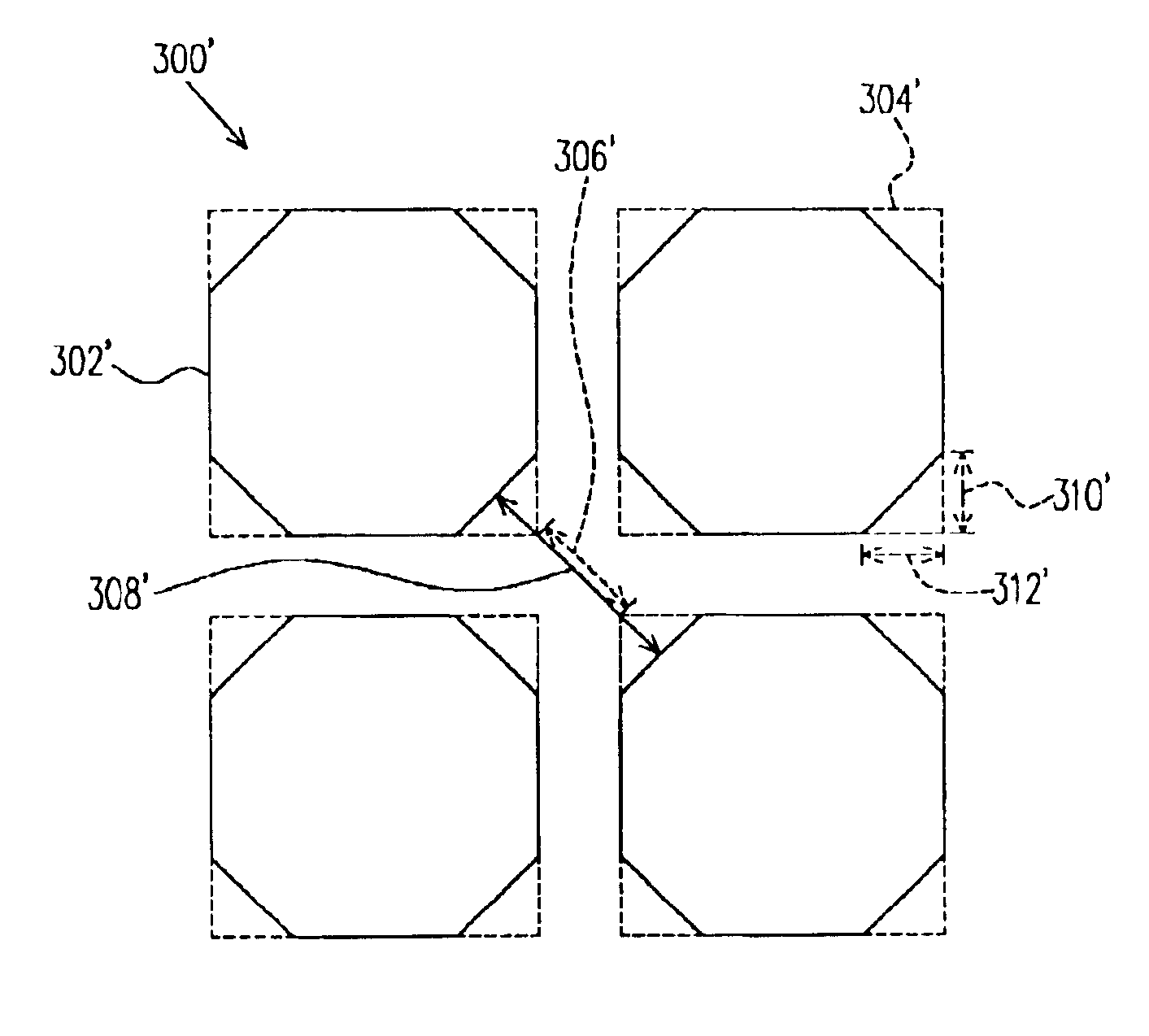
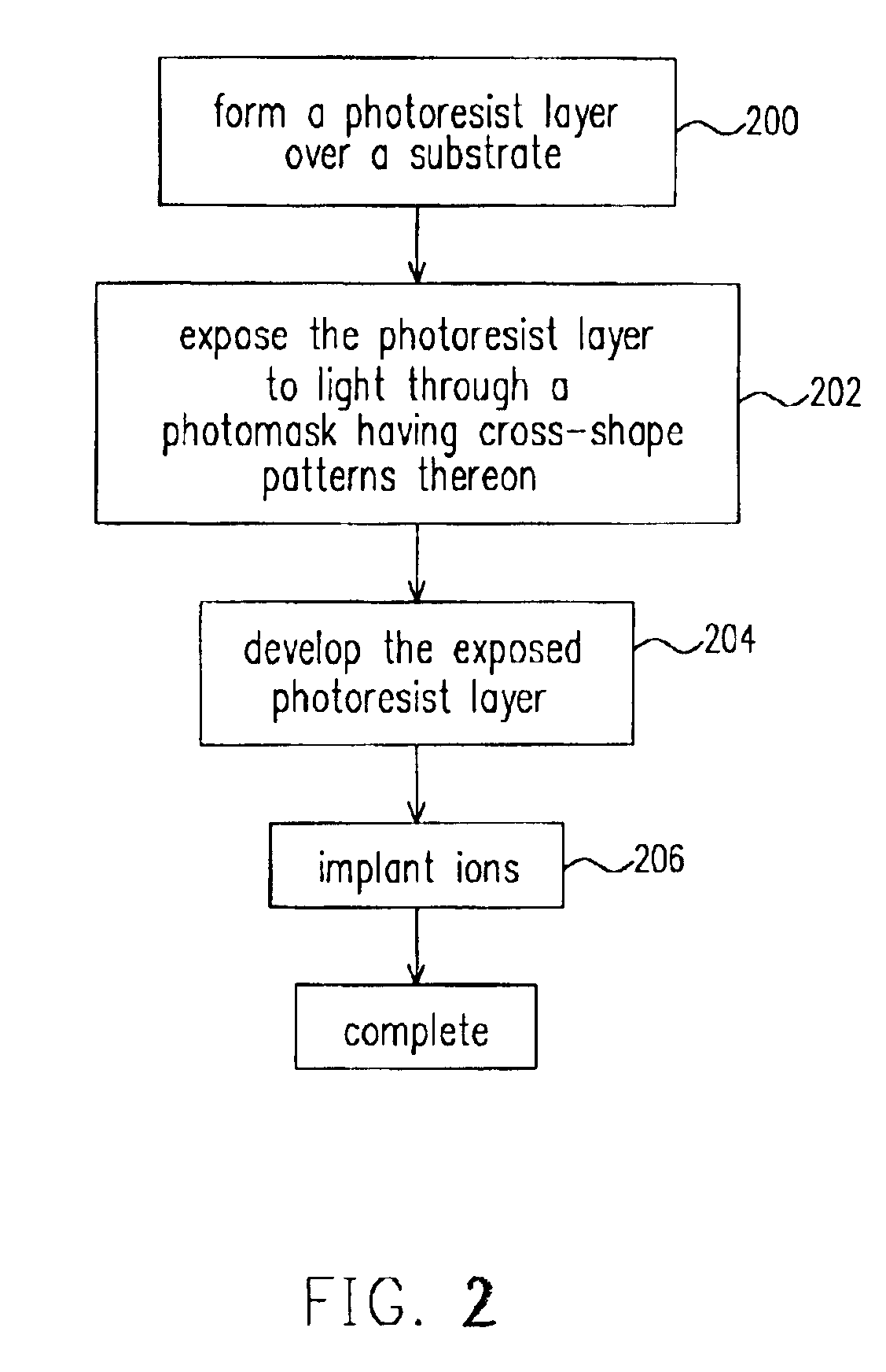
FIG. 2 is a flow chart showing the steps for forming holes in a layer through a a regular image with inwardly reduced corners, such as a cross-shape image exposure according to one preferred embodiment of this invention. In step 200, a photoresist layer is formed over a substrate. The substrate includes, for example, a semiconductor substrate, a semiconductor device, a conductive layer, a dielectric layer and so on. For example, a semiconductor device is formed over a semiconductor substrate and then a conductive layer that connects electrically with the semiconductor device is formed over the semiconductor substrate. A dielectric layer is formed over the semiconductor substrate covering the semiconductor ...


PUM


Abstract

A method of forming holes in a layer through a cross-shape image exposure. The method includes removing a section from each corner of the rectangular patterns on a photomask to form cross-shape patterns so that circular or elliptical contact holes are formed on a photoresist layer after photo-exposure and development. Optical image contrast between contacts is increased by the cross-shape patterns on the photomask.

Description

BACKGROUND OF INVENTION1. Field of InventionThe present invention relates to a method of forming holes. More particularly, the present invention relates to a method of forming holes in a layer through a cross-shape image exposure.2. Description of Related ArtIn recent years, many semiconductor manufacturers design circuit devices with the specific aim of miniaturization. One very important process in semiconductor production is photolithography. Size of critical dimension (CD) in many semiconductor device structures such as various thin film patterns depends on photolithographic processes. In other words, photolithographic process has tremendous impact the future development of semiconductor devices. The transfer of pattern through photomask is especially important because inaccuracy in pattern transfer is likely to affect tolerance of critical dimensions on a chip and lower exposure resolution.When a pattern on a photomask is transferred to a chip, proximity effect is a factor that...

Claims


Application Information

Patent Timeline
IPC IPC(8): G03F9/00G03C5/00H01L21/02H01L21/027H01L21/302H01L21/461H01L21/311G03F1/00G03F1/36H01L21/768
CPCG03F1/144G03F1/36H01L21/76802
Inventor WU, TSUNG-HSIENCHANG, CHING-YUYANG, TAHORNG
Owner MACORNIX INT
Why Eureka
Try Eureka