

Method of disposing conductive bumps onto a semiconductor device
- Summary
- Abstract
- Description
- Claims
- Application Information
AI Technical Summary
Benefits of technology
Problems solved by technology
Method used
Image

Examples
Embodiment Construction
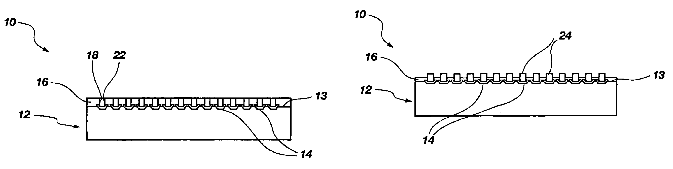
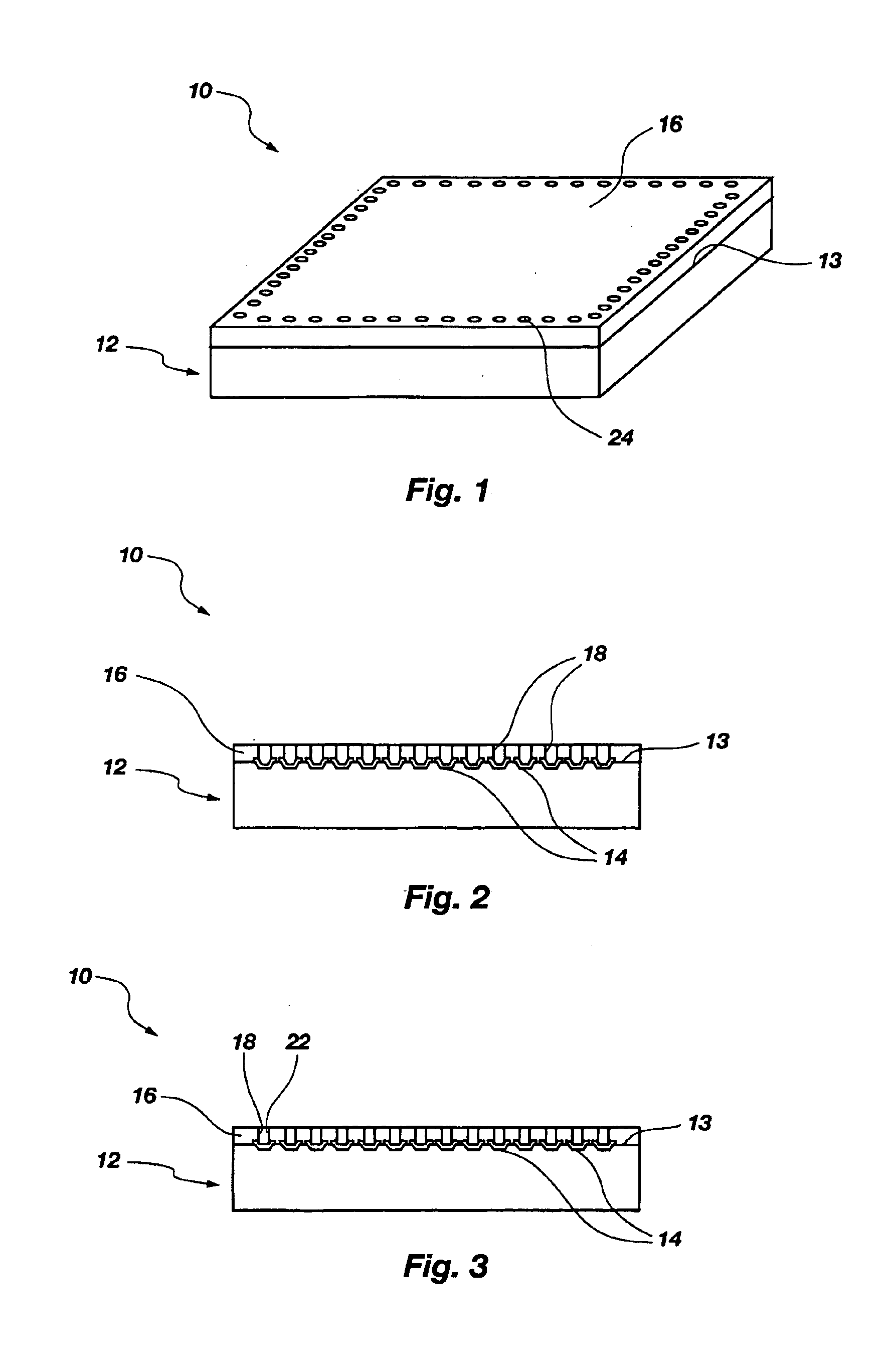
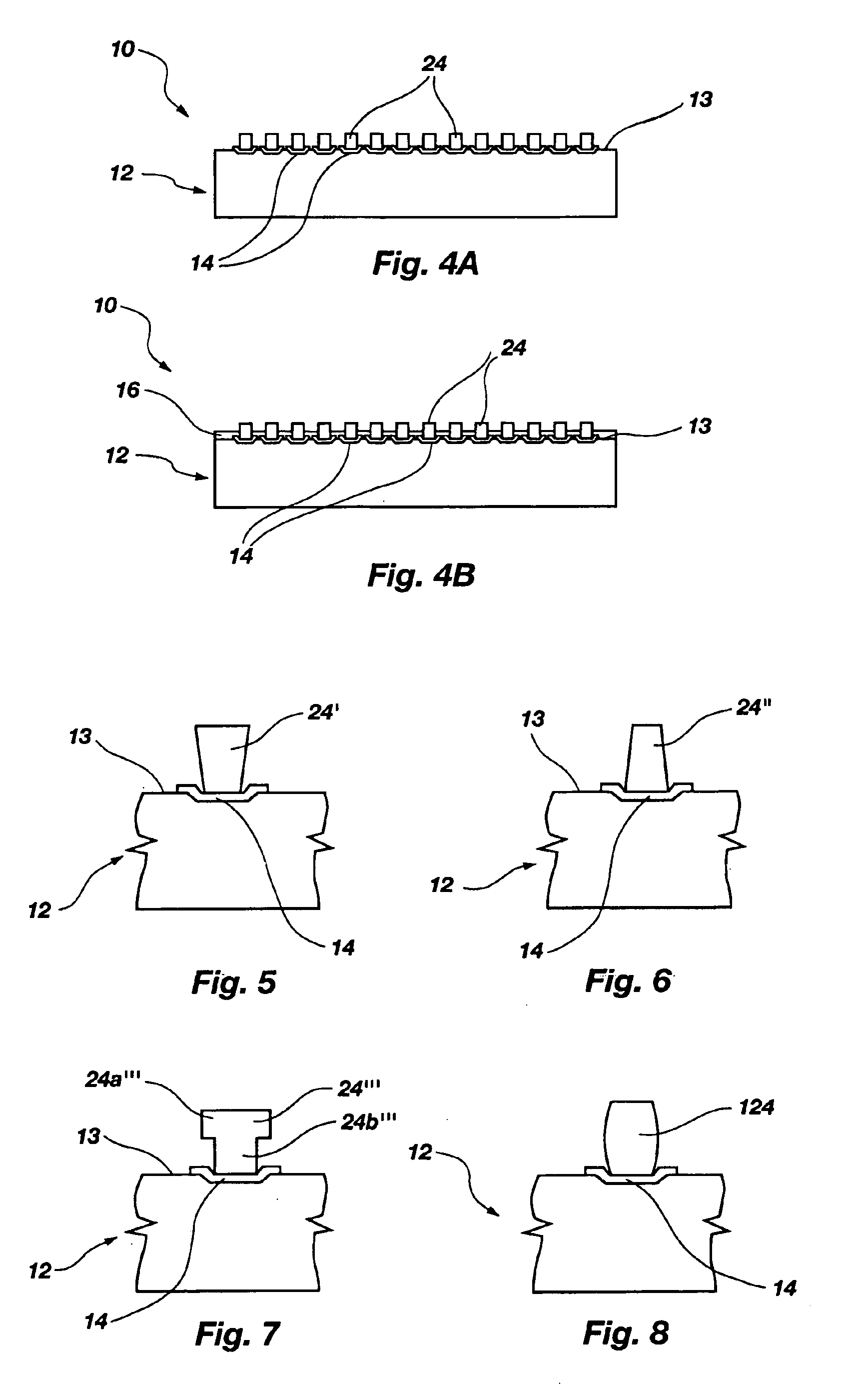
With reference to FIG. 1, a semiconductor device 10 according to the present invention, which includes a substrate 12 with integrated circuitry thereon and contact pads 14 (see FIGS. 2-8) in electrical communication with the integrated circuitry is illustrated. As depicted, substrate 12 is a semiconductor die and contact pads 14 are the bond pads of the semiconductor die. Typically and conventionally, the bond pads, when used with a tin / lead solder, may be coated with a plurality of superimposed metal layers to enhance the bonding of the solder to the metal of the bond pad. Further, contact pads may be offset from the bond pads and connected thereto by circuit traces extending over the active surface so as to rearrange an input / output pattern of bond pads to a pattern more suitable for an array of conductive bumps. Semiconductor device 10 also includes a solder mask 16 comprised of dielectric material disposed over an active surface 13 of substrate 12. Solder mask 16 includes apertu...
PUM
 Abstract
Description
Claims
Application Information