Semiconductor integrated circuit device and fabrication process thereof
- Summary
- Abstract
- Description
- Claims
- Application Information
AI Technical Summary
Benefits of technology
Problems solved by technology
Method used
Image
Examples
first embodiment
(First Embodiment)
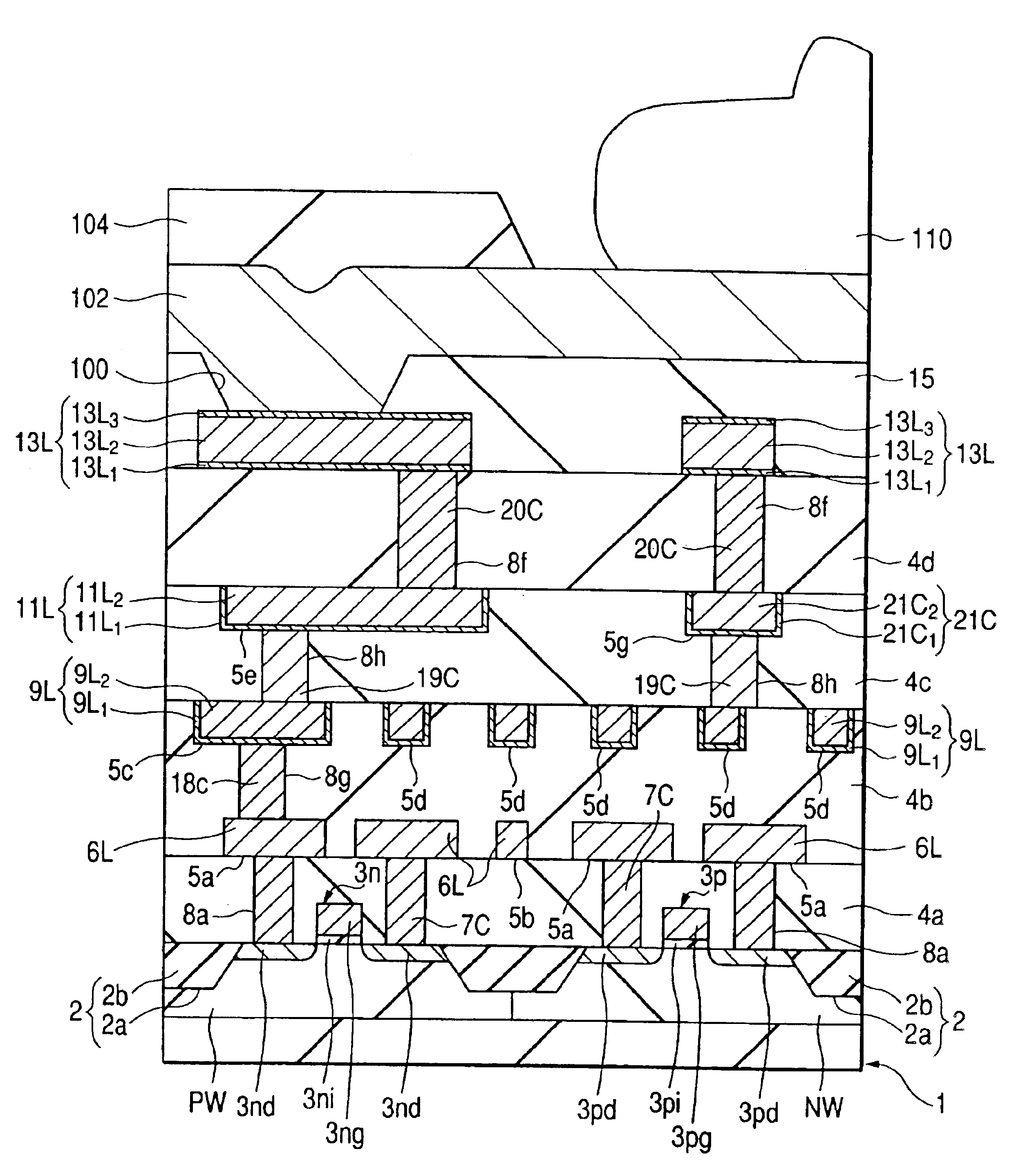
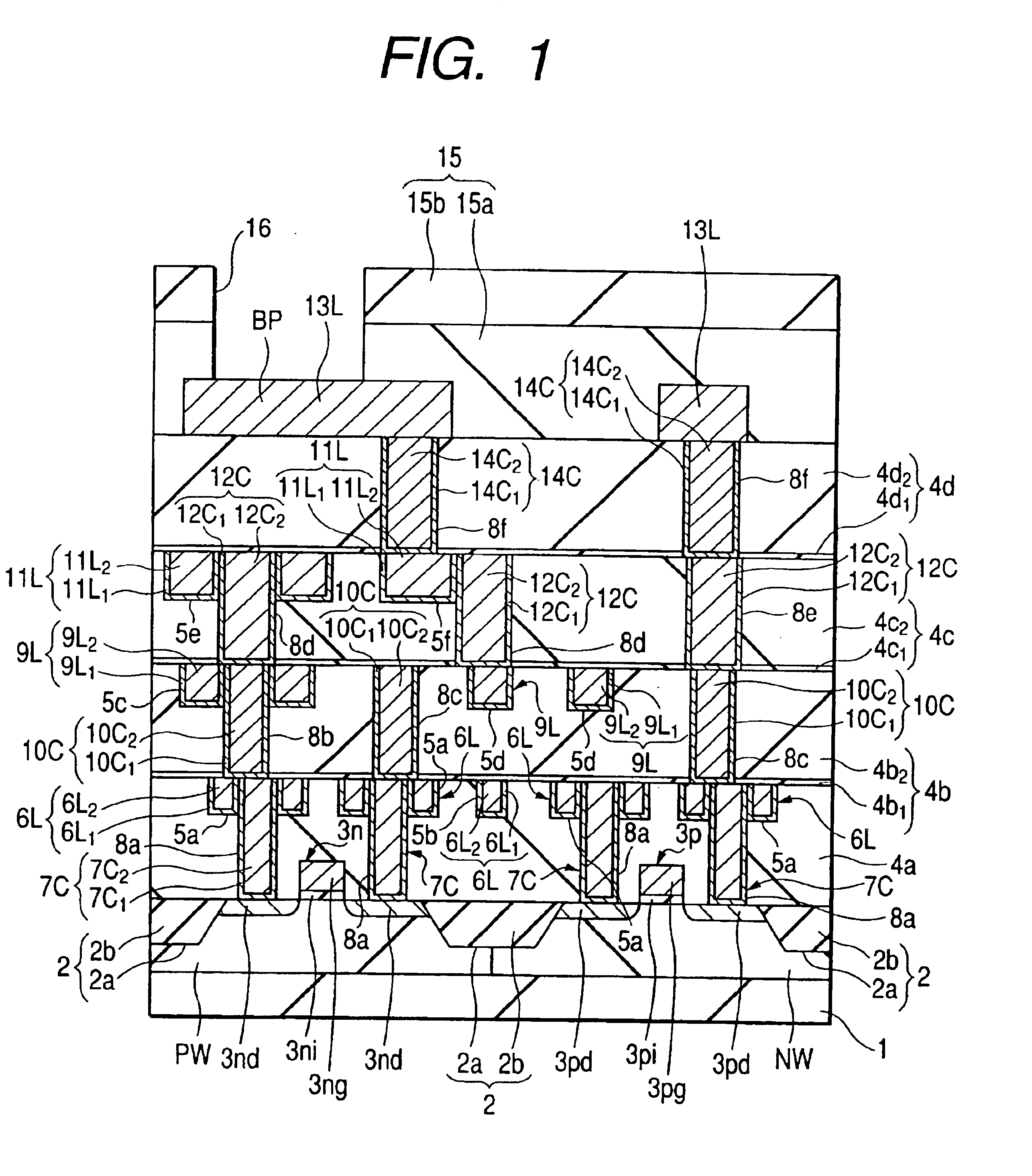
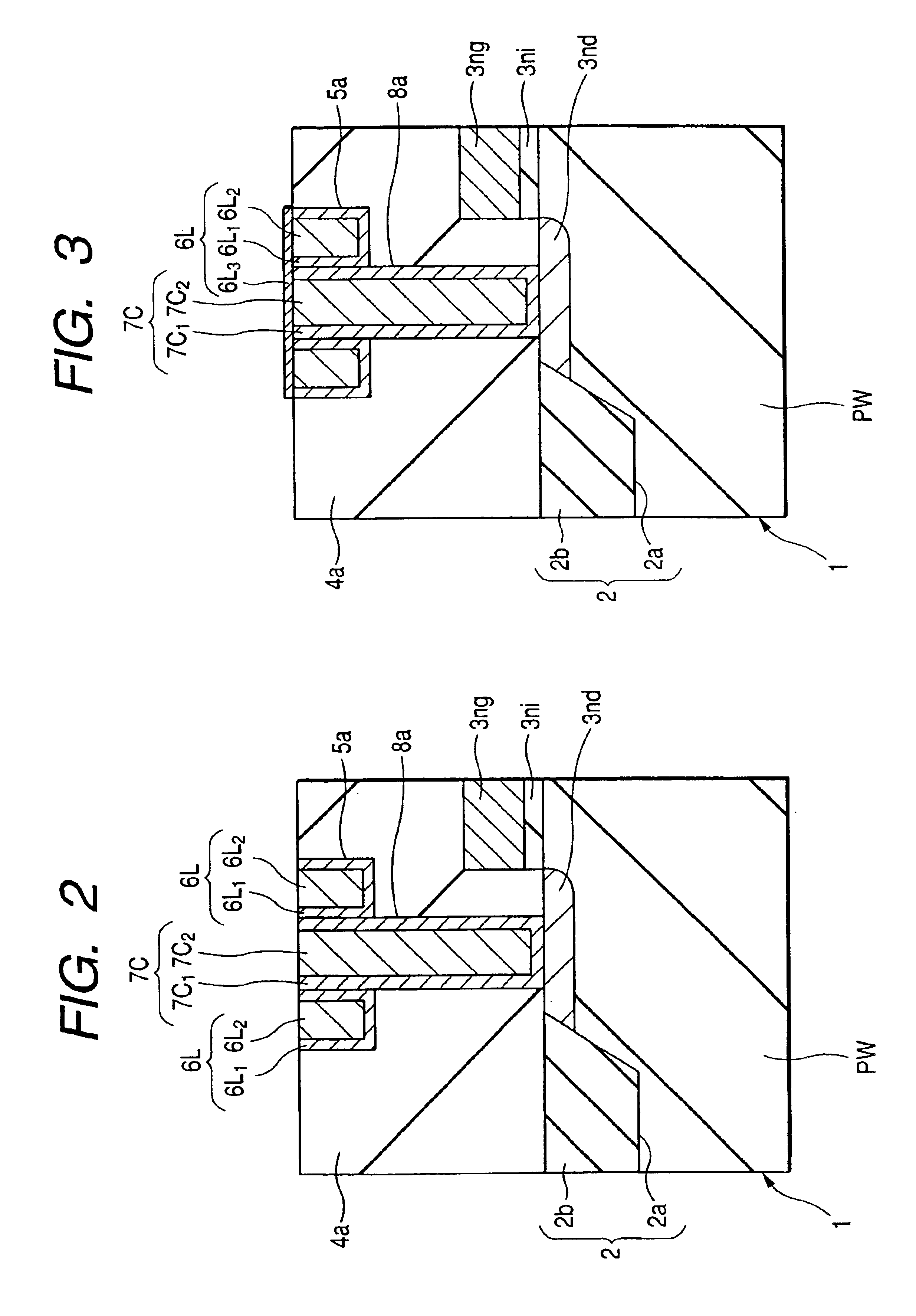
FIG. 1 is a fragmentary cross-sectional view of the semiconductor integrated circuit according to the first embodiment of the present invention; FIG. 2 is a fragmentary cross-sectional view illustrating the first-layer interconnection of the semiconductor integrated circuit device of FIG. 1; FIGS. 3 through 5 are cross-sectional views illustrating a modification of the interconnection structure of FIG. 2; FIG. 6 is a fragmentary cross-sectional view illustrating the second-layer interconnection of the semiconductor integrated circuit device of FIG. 1; FIG. 7 is a fragmentary cross-sectional view illustrating a modification of the connection between interconnection layers of the semiconductor integrated circuit device of FIG. 1; FIGS. 8 through 12 are fragmentary cross-sectional views of the semiconductor integrated circuit device of FIG. 1 during its fabrication process; and FIGS. 13 through 18 are fragmentary, partially-cutaway, perspective view of the semiconduct...
second embodiment
This second embodiment is different from the first embodiment in the structure of a connecting conductor portion and its forming process.
As illustrated in FIG. 19, a photoresist pattern 17b is formed on the upper surface of the interlayer insulating film 4a for the formation of an interconnection groove. Then, the interlayer insulating film 4a is etched with the photoresist pattern 17b as an etching mask, whereby an interconnection groove 5a is formed in the upper part of the interlayer insulating film 4a.
After the removal of the photoresist pattern 17b, a photoresist pattern 17c is formed, as illustrated in FIG. 20, over the interlayer insulating film 4a for the formation of a connecting hole. The interlayer insulating film 4a is etched with the photoresist pattern 17c as an etching mask, whereby a connecting hole 8a which extends toward the semiconductor substrate 1 from the bottom of the interconnection groove 5a and from which the upper surface of the semiconductor substrate 1 ...
third embodiment
(Third Embodiment)
FIGS. 25 through 28 and FIGS. 29 through 32 are fragmentary cross-sectional views of the semiconductor integrated circuit device according to the third embodiment of the present invention during the fabrication process; and FIG. 33 is a fragmentary cross-sectional view of the semiconductor integrated circuit device.
FIG. 25 illustrates the semiconductor integrated circuit device during the fabrication process. In the interlayer insulating film 4a, the interconnection groove 5a and connecting hole 8a are formed by the method as described in the second embodiment.
In the third embodiment, the connecting conductor portion 7C made of, for example, tungsten is formed in the connecting hole 8a by the selective CVD method as illustrated in FIG. 26. In this third embodiment, the film formation is carried out to such an extent as the upper part of the connecting conductor portion 7C protrudes outside the interconnection groove 5a. The material of the connecting conductor port...
PUM
 Abstract
Description
Claims
Application Information


