Active-matrix addressed reflective LCD and method of fabricating the same

a technology of active matrix and reflective lcd, which is applied in the direction of identification means, instruments, semiconductor devices, etc., can solve the problems of consuming considerable power, affecting the effect of reducing the intensity of exposing light, and affecting the processing steps of fabricating

Inactive Publication Date: 2005-03-01
NEC LCD TECH CORP
View PDF29 Cites 16 Cited by
  • Summary
  • Abstract
  • Description
  • Claims
  • Application Information

AI Technical Summary

Benefits of technology

In brief, these objects are achieved by the techniques wherein In order to improve processing steps of fabricating an active-matrix addressed reflective liquid crystal display, a lower substrate, which is positioned at one side with respect to a liquid crystal layer, is provided with two electrodes in parallel with each other and in parallel with the liquid crystal layer. One of the two electrodes is electrically coupled to a source electrode of a switching element assigned to one pixel, and the other electrode is electrically couple to a constant potential source. Each of the two electrodes has characteristics of light reflectivity, which is able to reduce the intensity of exposing light when an insulating layer provided above the electrodes is patterned.

Problems solved by technology

Although the transmissive LCD has many advantages, it has encountered the problems resulting from the presence of a built-in light source.
Namely, the transmissive LCD undesirably becomes bulky and consumes considerable power.
However, the active-matrix addressed reflective LCD according to the above-mentioned conventional technique has suffered from the following difficulties.
Therefore, the conventional technique suffers from the problems that the intensity of exposing light should be increased and the exposure time becomes long, which renders the fabrication processes complicated and undesirably increase the fabrication time of the device.
Second, the storage capacitance of each pixel is small, and thus, it is liable to induce flicker.
However, since each of the organic insulation layer 28 and the polyimide layer 11 has inherently a considerably large thickness in the case of an active-matrix addressed reflective LCD, and as such, it is difficult to realize sufficient storage capacitance.
As a result, it is difficult to achieve the expected irregularity on the surface of the reflection electrode 34.

Method used


Image

  • Active-matrix addressed reflective LCD and method of fabricating the same
  • Active-matrix addressed reflective LCD and method of fabricating the same
  • Active-matrix addressed reflective LCD and method of fabricating the same

Examples


Embodiment Construction

A preferred embodiment of the present invention will be described with reference to FIGS. 4 to 7I.

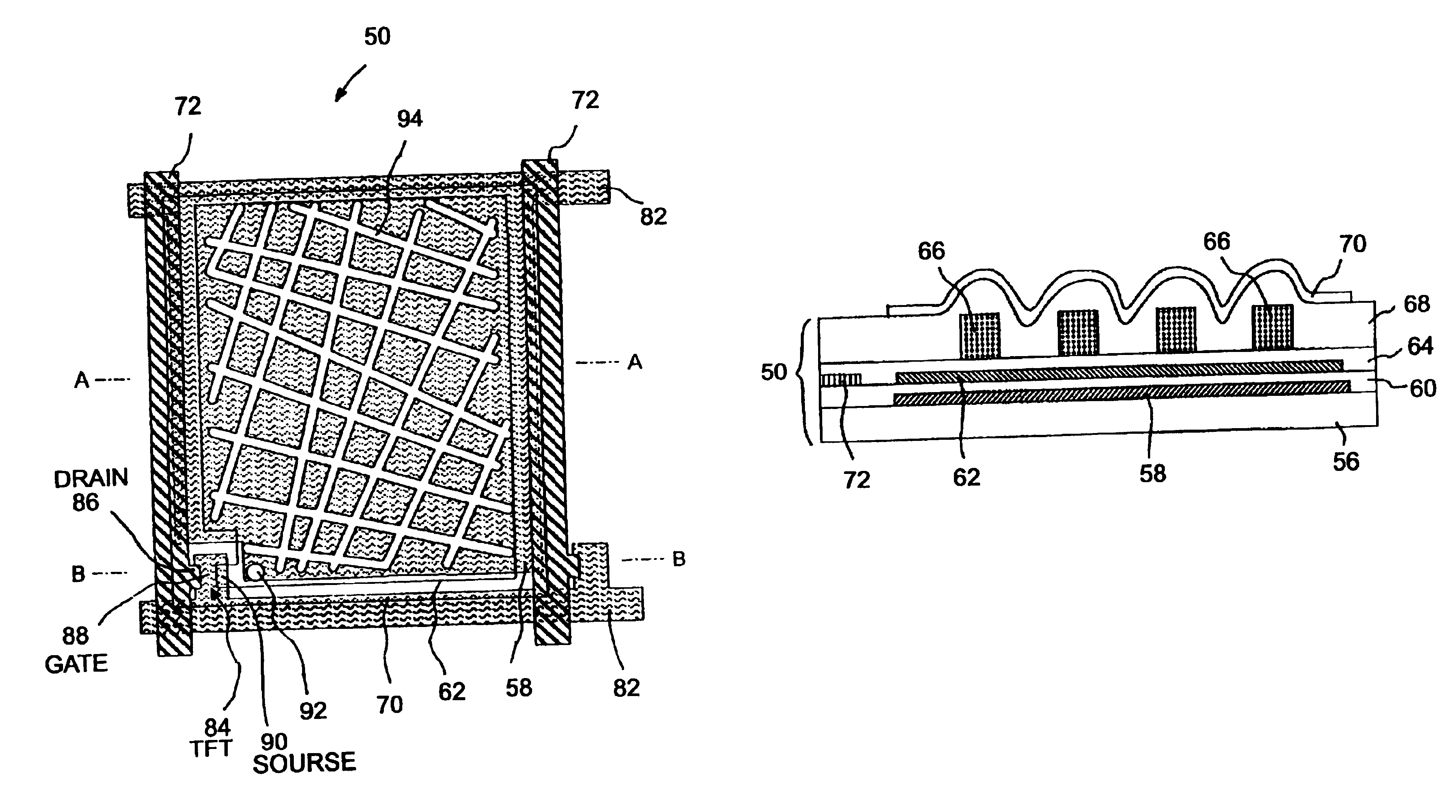
FIG. 3 is a sectional view of approximately one pixel area taken along a center line of the pixel, viz., along section line A—A of FIG. 4A, and thus, a switching element such as a thin film transistor is not shown in FIG. 3. The pixel area of FIG. 3 forms part of an active-matrix addressed reflective LCD according to the embodiment of the present invention.

The pixel area shown in FIG. 3 generally comprises a lower substrate 50, an upper substrate 52, and a liquid crystal layer 54 hermetically sealed between the substrates 50 and 52.

The lower substrate 50 is comprised of a glass substrate 56 on which a lower electrode 58 is provided. The lower electrode 58 is covered by a lower insulation film 60 that is also used as a gate insulation film of the thin film transistor (not shown in FIG. 3). An upper electrode 62 is deposited on the lower insulation film 60, and is covered by a passivation...


PUM

PropertyMeasurementUnit
heightsaaaaaaaaaa
heightsaaaaaaaaaa
thicknessaaaaaaaaaa

Abstract

In order to improve processing steps of fabricating an active-matrix addressed reflective liquid crystal display, a lower substrate, which is positioned at one side with respect to a liquid crystal layer, is provided with two electrodes in parallel with each other and in parallel with the liquid crystal layer. One of the two electrodes is electrically coupled to a source electrode of a switching element assigned to one pixel, and the other electrode is electrically couple to a constant potential source. Each of the two electrodes has characteristics of light reflectivity, which is able to reduce the intensity of exposing light when an insulating layer provided above the electrodes is patterned.

Description

BACKGROUND OF THE INVENTION1. Field of the InventionThe present invention relates generally to an active-matrix addressed liquid crystal display (LCD), and more specifically to such an LCD having a reflective electrode via which ambient light as the reading source is reflected thereby and again emitted out of the device. Still more specifically, the present relates to a method of fabrication such an LCD.2. Description of Related ArtLCDs have found extensive uses in a variety of electronic devices such as television receivers, personal computers, personal digital assistances (PDAs), mobile telephone terminals, picture monitors, and so on. Among others, active-matrix addressed LCDs have widely utilized, which are provided with a plurality of active elements (switching elements) respectively assigned to pixel electrodes for controlling application of voltages thereto. The active element is typically a thin film transistor (TFT) or a metal-insulator-metal (MIM) diode. The active-matrix ...

Claims


Application Information

Patent Timeline
Patent Type & Authority Patents(United States)
IPC IPC(8): G02F1/1335G02F1/13G02F1/1362G02F1/1368G09F9/00G09F9/30H01L21/336H01L29/786
CPCG02F1/136213G02F1/133553G02F1/1335
Inventor SAKAMOTO, MICHIAKIYAMAGUCHI, YUICHIIKENO, HIDENORIMATSUNO, FUMIHIKOKIKKAWA, HIRONORI
Owner NEC LCD TECH CORP
Why Eureka
Try Eureka