Optical waveguide element, manufacturing method for optical waveguide element, optical deflecting element, and optical switching element

a manufacturing method and waveguide technology, applied in the direction of optical waveguide light guide, optical waveguide, optics, etc., can solve the problems of increased coupling loss with optical fiber, no fine pattern production technique available, and difficult to fabricate optical waveguide in flared shape, so as to reduce coupling loss and facilitate layer shape

Inactive Publication Date: 2005-03-01
EPIPHOTONICS CORP
View PDF15 Cites 25 Cited by
  • Summary
  • Abstract
  • Description
  • Claims
  • Application Information

AI Technical Summary

Benefits of technology

[0018]Thus, by providing a cladding layer whose refractive index is smaller than that of the optical waveguide layer over the optical waveguide it is made possible to expand the diameter of the mode field in the optical waveguide and thereby substantially reduce the coupling loss between the optical fiber and the optical waveguide element. Furthermore, the shape of the cladding layer whose thickness gradually increases towards the end(s) over at least one of the incidence end and the emission and of the optical waveguide can also help reduce to light propagation loss in the optical waveguide element to a negligible level.
[0019]The manufacturing method for optical waveguide elements according to another aspect of the invention, make it easier to shape the layer and enables optical waveguide elements to be produced more precisely than where a thin film obtained by solid phase epitaxial growth is shaped, because first an amorphous thin film having a smaller refractive index than that of the optical waveguide layer is formed over the surface of the optical waveguide layer provided with an optical waveguide, then this amorphous thin film is so shaped as to leave a flared part whose thickness increases towards the end(s) over at least one of the incidence end and the emission end of the optical waveguide, and the shaped amorphous thin film is further formed into a flared shape through solid phase epitaxial growth by heating.
[0020]Another manufacturing method for optical waveguide elements according to still another aspect of the invention, make possible, in addition to the formation of the cladding layer in the same manner as the foregoing manufacturing method for optical waveguide elements, shaping of an amorphous thin film formed over the surface of the monocrystalline substrate into a prescribed channel pattern, formation of the shaped amorphous thin film into a buffer layer by solid phase epitaxial growth, and formation of a channel optical waveguide through solid phase epitaxial growth of an optical waveguide layer over this buffer layer, resulting in an optical waveguide element having a fine pattern of the channel optical waveguide, whose side walls and surface are smooth and which is hardly susceptible to scattering loss.

Problems solved by technology

Hei 7-78508), but an epitaxially grown thin film optical guide often has to be thinner than the mode field diameter of the optical fiber on account of the requirement for singleness of the mode or that to reduce the drive voltage, inviting an increased loss in coupling with the optical fiber.
However, there is no technique available for producing a fine pattern in the epitaxially grown oxide thin film optical waveguide, making it difficult to fabricate the optical waveguide in a flared shape.
For silica-based optical waveguides and the like, a method for producing channel optical waveguides by reactive ion etching is disclosed by Kawachi in NTT R&D, 43 (1994)1273 and elsewhere, but it is difficult to accomplish selectively etch a monocrystalline epitaxial ferroelectric thin film optical waveguide without roughing its surface, which would invite scattering loss or damaging the substrate, which is an oxide of the same kind as the thin film optical waveguide.
Furthermore, there is another problem that merely flaring an epitaxially grown oxide thin film optical waveguide can hardly prevent the waveguide mode from becoming multi-mode.

Method used


Image

  • Optical waveguide element, manufacturing method for optical waveguide element, optical deflecting element, and optical switching element
  • Optical waveguide element, manufacturing method for optical waveguide element, optical deflecting element, and optical switching element
  • Optical waveguide element, manufacturing method for optical waveguide element, optical deflecting element, and optical switching element

Examples


second embodiment

profiles illustrating the manufacturing process of the optical waveguide element, which is the invention;

[0033]FIG. 12 is a perspective view of the configuration of an optical switching element, which is a third embodiment of the invention;

[0034]FIG. 13 is a perspective view of the configuration of an optical deflection element, which is a fourth embodiment of the invention;

[0035]FIGS. 14A through 14D illustrates variations of the flare structure;

[0036]FIG. 15 is a perspective view of a variation of the optical waveguide element, which is the first embodiment of the invention; and

[0037]FIG. 16 is a perspective view of another variation of the optical waveguide element which is the first embodiment of the invention.

DETAILED DESCRIPTION OF THE PREFERRED EMBODIMENTS

[0038](First Embodiment)

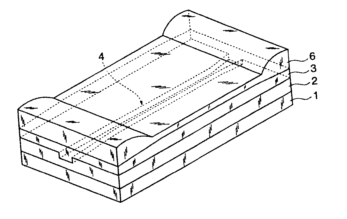
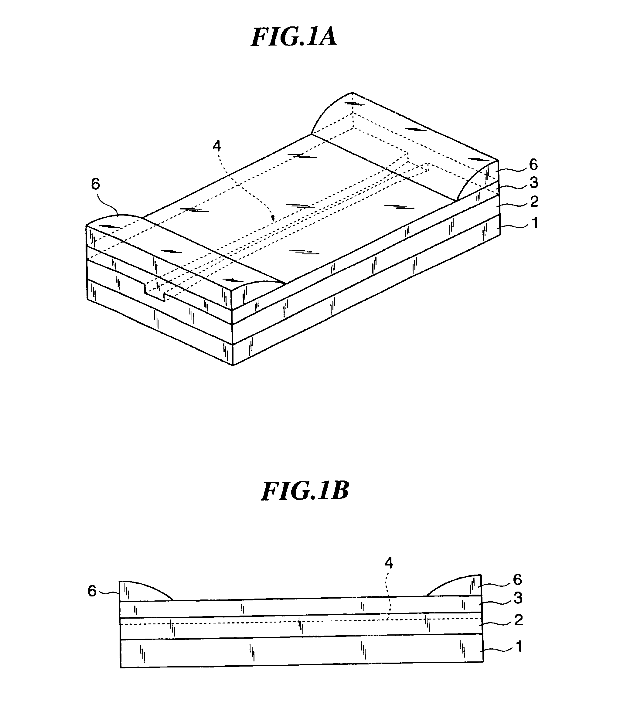
[0039]The optical waveguide element, which is the first embodiment of the invention, will be described. As illustrated in FIGS. 1A and 1B, this optical waveguide element is provided with a buffer laye...


PUM

PropertyMeasurementUnit
widthaaaaaaaaaa
mode field diameteraaaaaaaaaa

Abstract

An optical waveguide element capable of being coupled with optical fibers at high coupling efficiency is to be provided. Also an optical waveguide element manufacturing method permitting accurate production of such optical waveguide elements is to be provided. The optical waveguide element is provided with a buffer layer formed over a monocrystalline substrate and an optical waveguide layer formed over the buffer layer, and a recess is formed in the buffer layer along the lengthwise direction of the monocrystalline substrate. The optical waveguide layer is provided to fit into this recess to form a channel optical waveguide. Over the upper face of the optical waveguide layer on the light incidence side and the light emission side, a cladding layer whose refractive index is smaller than that of the optical waveguide layer and whose thickness increases towards the end face(s) in a flared shape is provided in the same width as that of the monocrystalline substrate. By providing the cladding layer whose refractive index is smaller than that of the optical waveguide layer, it is made possible to expand the mode field diameter and substantially reduce the coupling loss between the optical fiber and the optical waveguide element. Further by increasing the thickness of the cladding layer in a flared shape toward the end face(s), it is made possible to gradually compress the mode field diameter and to reduce the optical propagation loss within the optical waveguide.

Description

BACKGROUND OF THE INVENTION[0002]1. Field of the Invention[0003]The present invention relates to an optical guide waveguide element, a manufacturing method for optical waveguide elements, an optical deflection element and an optical switching element, and more particularly to an optical waveguide element capable of being coupled with an optical fiber at high coupling efficiency and a manufacturing method for such optical waveguide elements, an optical deflection element and an optical switching element to which the optical waveguide element according to the invention is applied.[0004]2. Description of the Related Art[0005]Conventionally, glass such as silica, oxide ferroelectrics and electro-optical materials such as LiNbO3, magneto-optical materials such as Y3Ga5O12, polymers such as PMMA, and GaAs-based chemical compound semiconductors are used for planar optical waveguides. Among those materials, oxide ferroelectrics are known to manifest particularly satisfactory acousto-optical...

Claims


Application Information

Patent Timeline
Patent Type & Authority Patents(United States)
IPC IPC(8): G02F1/055G02F1/01G02B6/13G02B6/136G02B6/30G02B6/12G02B6/122G02F1/035G02F1/295G02F1/313
CPCG02B6/1228G02B6/131G02F1/0553G02B6/305G02B6/136G02B2006/12145
Inventor NASHIMOTO, KEIICHI
Owner EPIPHOTONICS CORP
Why Eureka
Try Eureka