
Apparatus and method for testing memory in a microprocessor

Inactive Publication Date: 2005-03-01
IP FIRST
View PDF5 Cites 33 Cited by
  • Summary
  • Abstract
  • Description
  • Claims
  • Application Information

AI Technical Summary

Benefits of technology

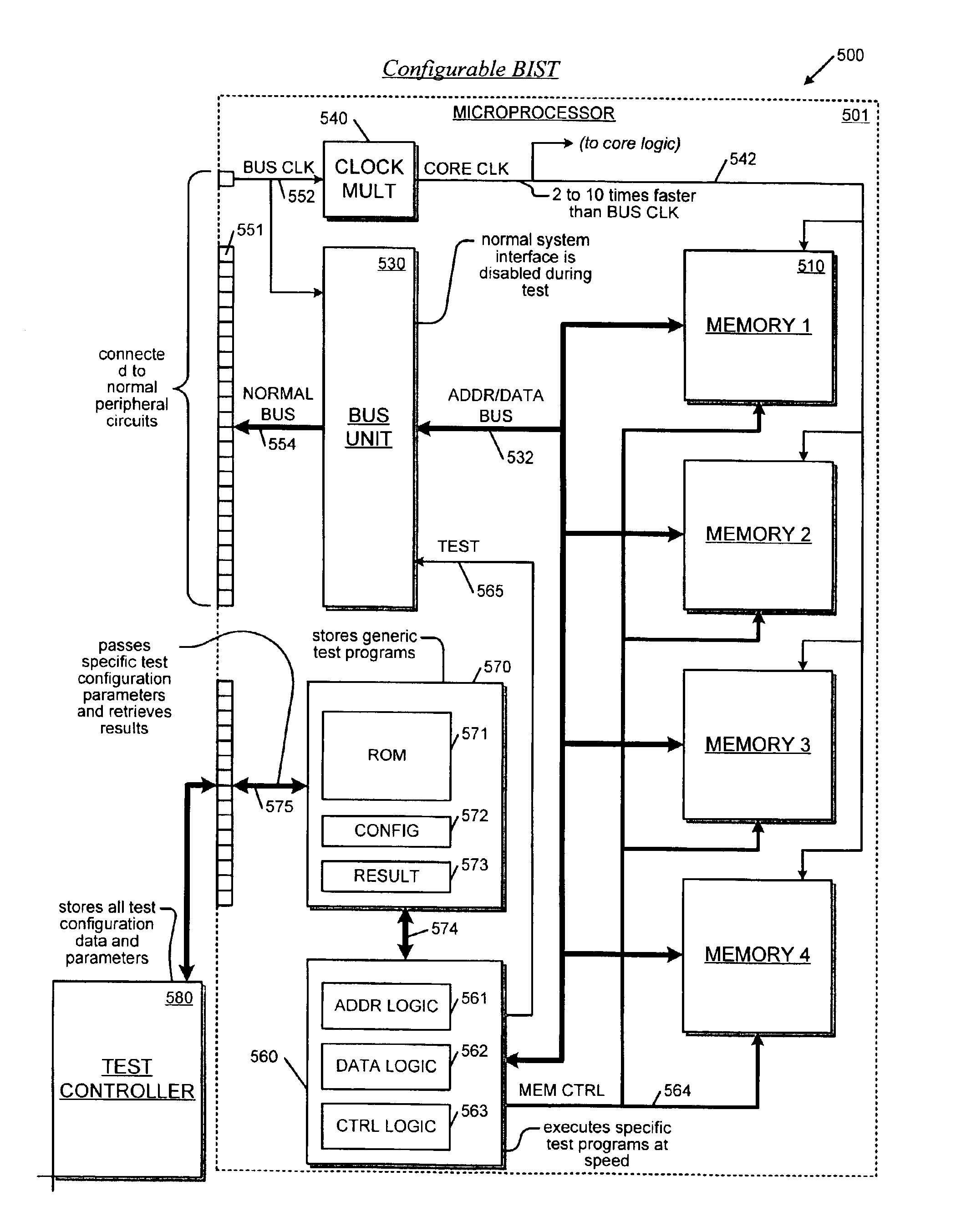
An advantage of the present invention is that full speed testing can be performed on memories in a microprocessor without having to sacrifice the ability to configure test sequences that were not originally designed into the device.
is that full speed testing can be performed on memories in a microprocessor without having to sacrifice the ability to configure test sequences that were not originally designed into the device.
An additional advantage of the present invention is that information is collected during memory testing to facilitate memory array repair.
Another object of the present invention is to provide a configurable memory test apparatus within a microprocessor that can accept test parameters from a chip tester.
In another aspect, it is a feature of the present invention to provide an apparatus for testing memory in a microprocessor. The apparatus has a test controller, test management logic, and test execution logic. The test controller provides test parameters to the microprocessor to configure a specific test program. The test management logic is within the microprocessor and is coupled to the test controller. The test management logic accepts the test parameters and generates the specific test program, where the specific test program is generated from a non-specific test program by insertion of the test parameters in place of a plurality of non-specific test operands. The test execution logic is within the microprocessor and is coupled to the test management logic. The test execution logic executes the specific test program.
Another advantage of the present invention is that chip tester programs, because they only pass test parameters to a microprocessor, are less complex and utilize less of the tester's resources. Only a small amount of memory within a chip tester is required.

Problems solved by technology

But, the additional logic devices, in order to route the signals to the external pins, are unavoidably designed directly into the primary internal path of the signals, thus introducing delays into both test mode operation and normal mode operation of the microprocessor.
More precisely, the delays caused by additional direct access routing logic in the microprocessor prevent testing of its memories at full speed.
But, more importantly, the delays slow down its normal operation.
Consequently, while direct access testing provides the capability to configure virtually any test sequence, the inherent delays imposed by the additional logic slows down the normal operation of the device and allows a notable number of defects to go undetected, because the memories cannot be tested at full speed.
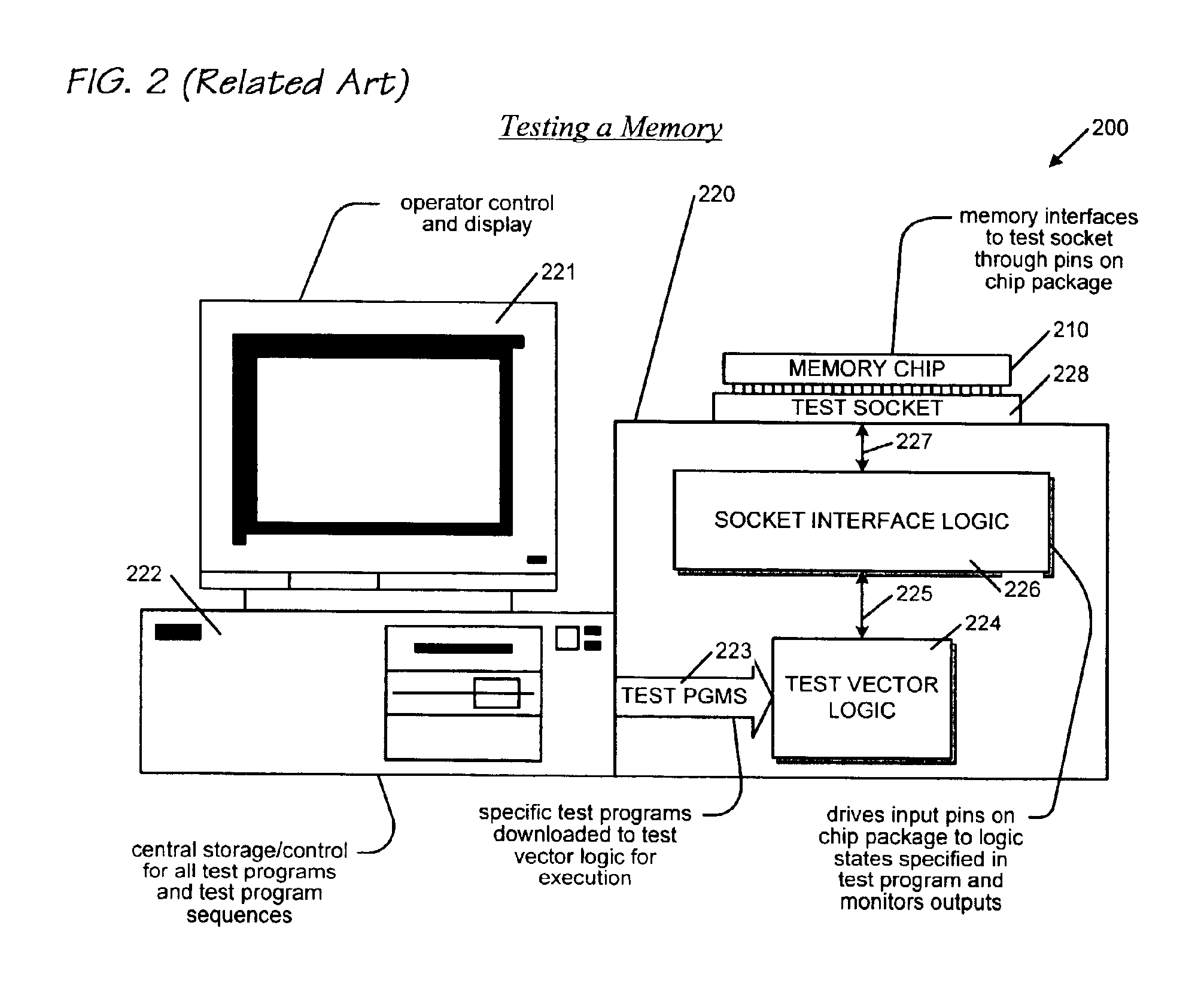
Another negative side effect of the direct access method is that a large amount of (very expensive) chip tester vector memory is required to store the different data patterns that are required to write to and read from the memory array.
This BBIST logic also consumes silicon area and power that is essentially wasted in normal use since it is only useful during chip manufacturing testing.

Method used


Image

  • Apparatus and method for testing memory in a microprocessor
  • Apparatus and method for testing memory in a microprocessor
  • Apparatus and method for testing memory in a microprocessor

Examples


Embodiment Construction

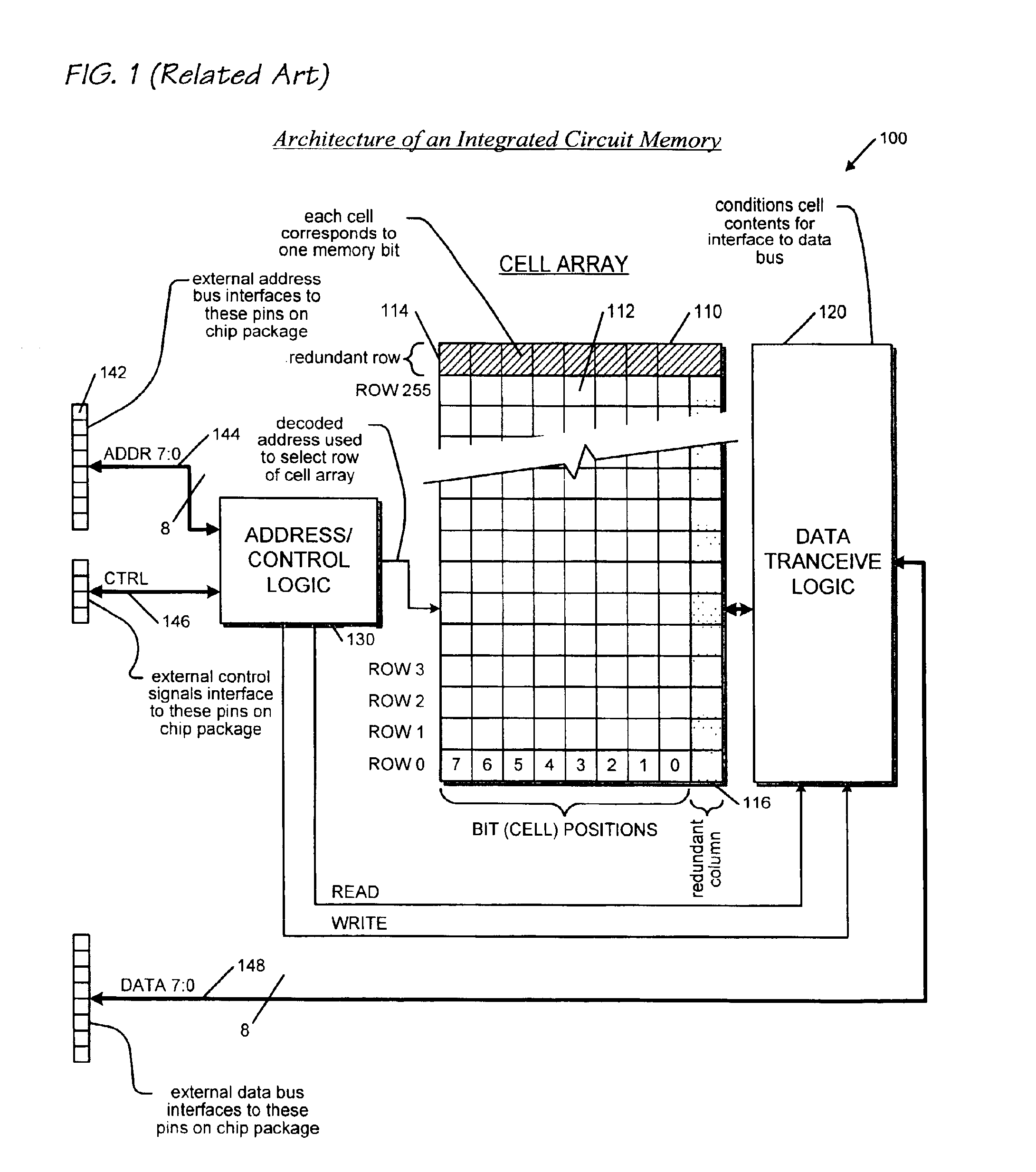
Several related art examples with respect to memory testing will now be described with reference to FIGS. 1 through 4. These examples illustrate the problematic nature of present day memory testing techniques, particularly when it is desired to test memories at full speed within a microprocessor, yet when configurability of test parameters is also required. Following this discussion, a detailed description of the present invention will be provided with reference to FIGS. 5 through 7. Use of the present invention provides both the flexibility to configure specific parameters for testing memories in a microprocessor and allows for memory array repair without consuming excessive tester resources. The present invention moreover provides the ability to test those memories at full speed without compromising full speed operation of the microprocessor when it is in a normal mode of operation.

Now referring to FIG. 1, a diagram is presented illustrating the architecture of a related art memor...


PUM


Abstract

An apparatus and method are provided for testing memory circuits in a microprocessor. The apparatus includes test management logic and test execution logic located within the microprocessor. The test management logic has a non-specific test program stored therein, and it accepts test parameters provided by an external test controller. The test parameters are applied to the non-specific test program to produce a specific test program by inserting the test parameters in place of a plurality of non-specific test operands. The test execution logic executes the specific test program to test the memory circuits within the microprocessor at the internal speed of the microprocessor.

Description

BACKGROUND OF THE INVENTION1. Field of the InventionThis invention relates in general to microprocessor design and manufacture, and more particularly to an apparatus and method for testing memory circuits in a microprocessor.2. Description of the Related ArtTwo techniques are primarily employed to test memories in a microprocessor: the direct access technique and the built in self test (BIST) technique.The direct access technique utilizes additional logic devices within the microprocessor to route all essential signals required for testing internal memories out to exterior pins on the operational package of the microprocessor. Thus, when the microprocessor is installed in a chip tester, the additional logic routes the address / data / control signals for a designated memory directly to external pins, thus bypassing internal circuitry that would otherwise preclude access to the signals. As a result, the chip tester is able to configure and execute any desired test sequence to detect defe...

Claims


Application Information

Patent Timeline
IPC IPC(8): G11C29/12G11C29/48G11C29/56G11C29/04
CPCG11C29/12G11C29/56G11C29/48
Inventor MINER, DANIEL G.
Owner IP FIRST
Learn More