Wire bonding process and wire bond structure

a wire bonding and wire bonding technology, applied in the direction of auxillary welding devices, soldering apparatus, semiconductor/solid-state device details, etc., can solve the problem of reducing the reliability of the electronic packaging structure, and achieve the effect of improving the reliability of the packaging structure and improving the quality of the electrical connection

Inactive Publication Date: 2005-03-08
ADVANCED SEMICON ENG INC
View PDF8 Cites 19 Cited by
  • Summary
  • Abstract
  • Description
  • Claims
  • Application Information

AI Technical Summary

Benefits of technology

An aspect of the invention therefore is to provide a wire-bonding process and a wire-bonding structure that can improve the quality of the electrical connection through bonding-wires, which thus improves the reliability of packaging structures.

Problems solved by technology

As a result, the reliability of the electronic packaging structure is reduced.

Method used


Image

  • Wire bonding process and wire bond structure
  • Wire bonding process and wire bond structure
  • Wire bonding process and wire bond structure

Examples


first embodiment

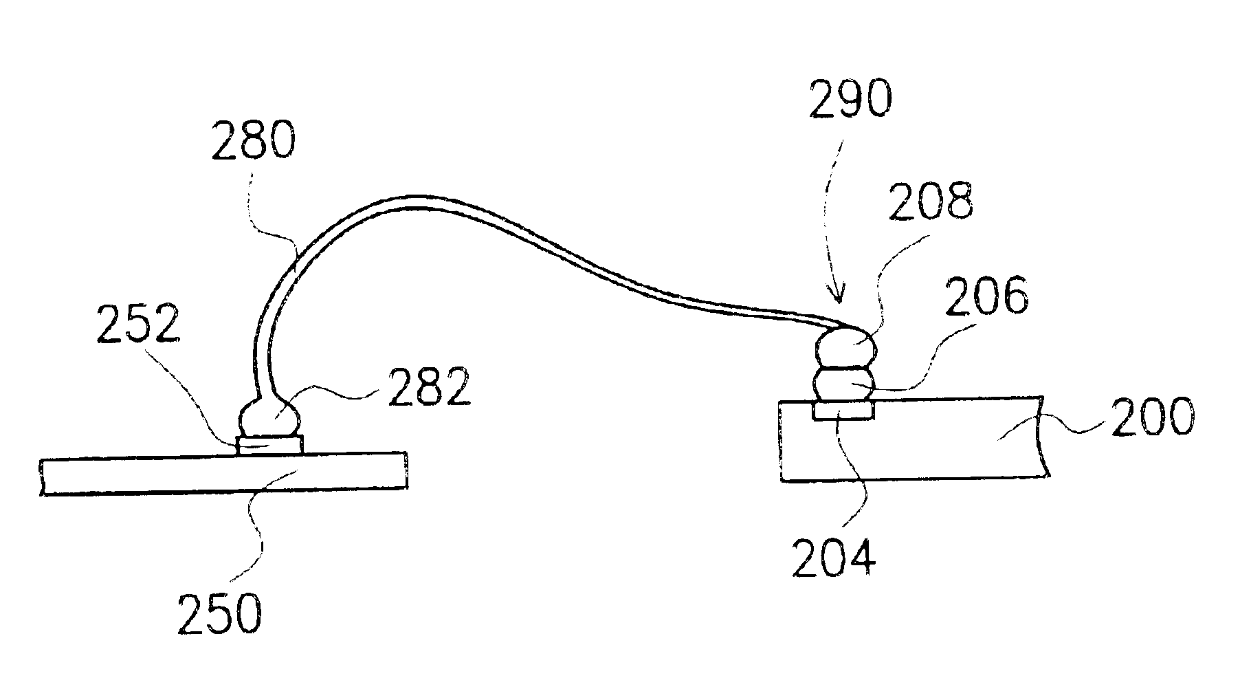
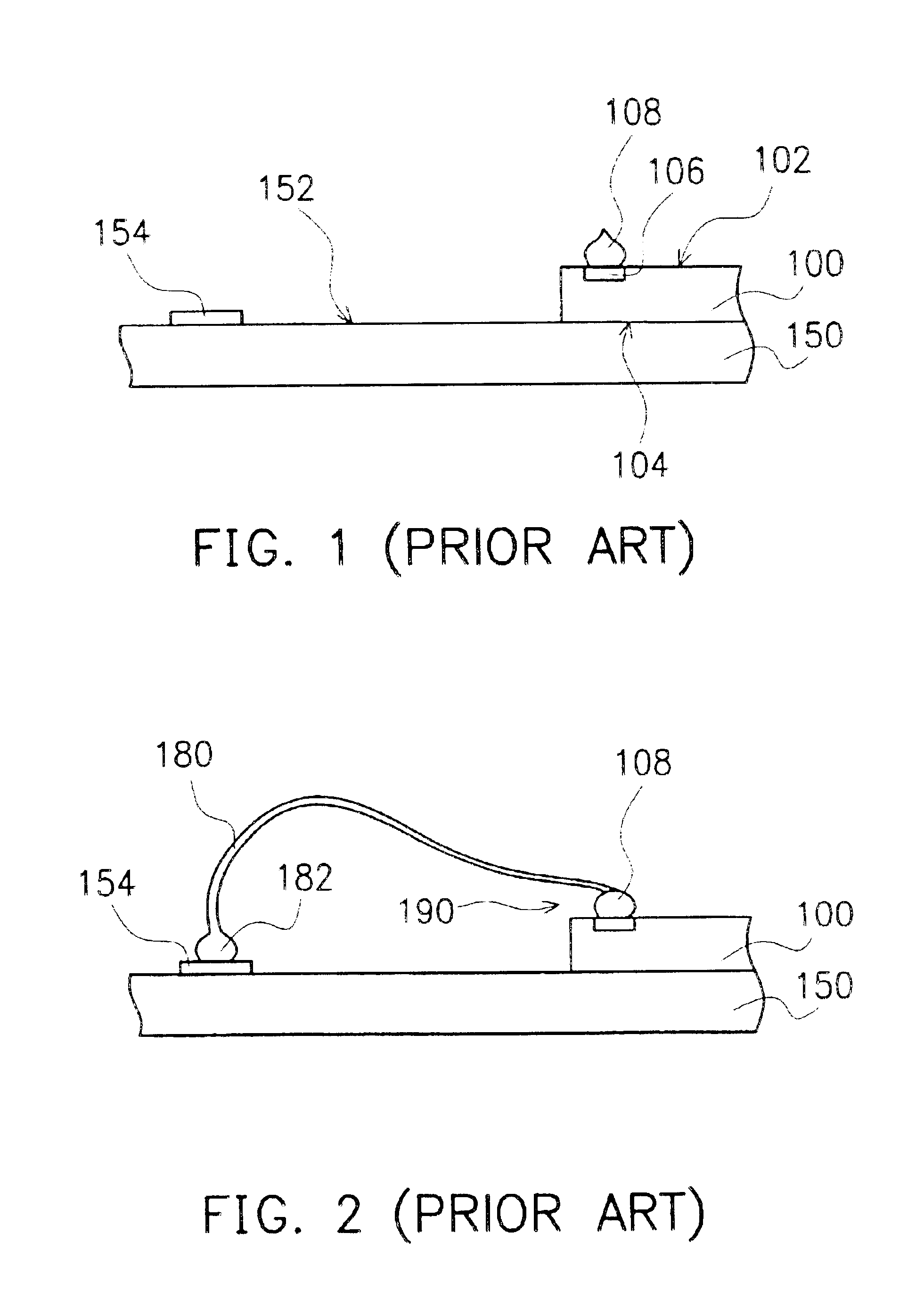
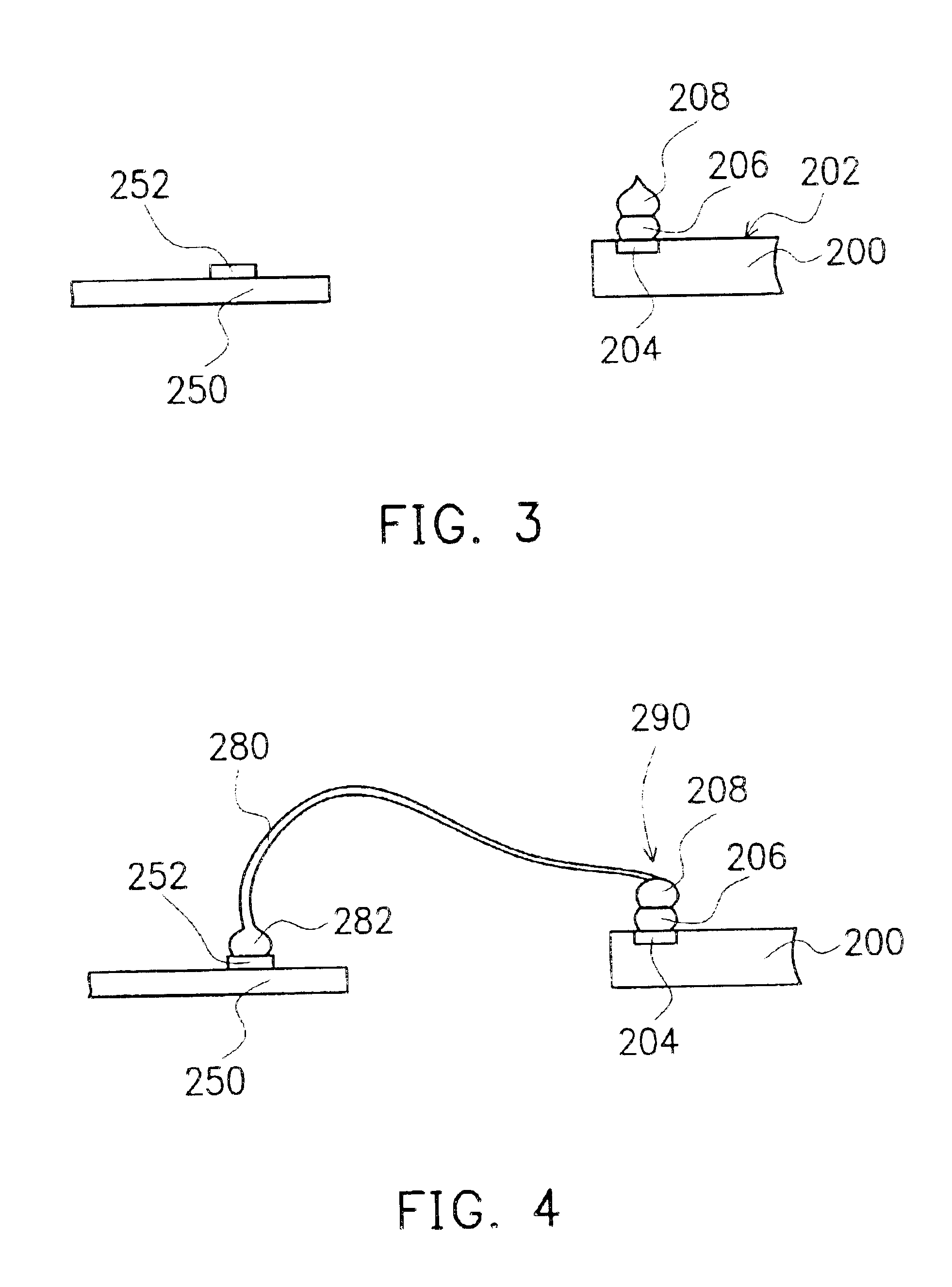
Referring to FIG. 3 and FIG. 4, cross-sectional views schematically illustrate a wire-bonding process according to the present invention.

With reference to FIG. 3, a chip 200 is provided with an active surface 202 on which are formed at least a first contact pad 204. A chip carrier 250 further includes at least a second contact pad 252 thereon. A plurality of stacked bumps (206, 208) are formed on the first contact pad 204 through, for example, up-down movements of a wire-bonding machine head releasing the conductive material that forms the bumps. In the present description, reference numeral 206 refers to the bump that is formed on the contact pad 204 and reference numeral 208 refers to the uppermost bump.

Referring to FIG. 4, a reverse bonding process is performed as described hereafter. First, a prominence 282 is formed on the second contact pad 252 of the chip carrier 250 in ball-bonding fashion. Then, while moving from the second contact pad 252 to the stacked bumps (206, 208), t...

second embodiment

Referring now to FIG. 5 and FIG. 6, cross-sectional views schematically illustrate a wire-bonding process of the present invention.

Referring to FIG. 5, a chip 300 is provided with an active surface 302 on which at least a first contact pad 304 is formed. A chip carrier 350 is further provided with at least a second contact pad 352 thereon. A first bump 306 is formed on the first contact pad 304 by way of, for example, vertical up and down movements of a wire-bonding machine head releasing a conductive material to form the bump.

Referring to FIG. 6, a reverse bonding process is performed as follows. First, a prominence 382 is formed on the second contact pad 352 of the chip carrier 350 in ball-bonding fashion. Then, while moving from the second contact pad 352 to the first bump 306, the wire-bonding machine head continuously releases a conductive material to form a conductive wire 380 hence bonded to the first bump 306 in stitch-bonding fashion. A second bump 308 then is formed on th...


PUM

PropertyMeasurementUnit
conductiveaaaaaaaaaa
structureaaaaaaaaaa
electricalaaaaaaaaaa

Abstract

In a wire-bonding process, a chip is provided with at least a first contact pad. A chip carrier is further provided with at least a second contact pad. A plurality of stacked conductive bumps are formed on the first contact pad. A conductive wire is formed by a reverse bonding process. The conductive wire electrically connects the second contact pad of the chip carrier to the stacked conductive bumps over the first contact pad of the chip.

Description

BACKGROUND OF THE INVENTION1. Field of the InventionThe invention relates to a wire bonding process and a wire-bonding structure. More particularly, the invention relates to a wire-bonding process performed according to reverse bonding fashion.2. Description of the Related ArtAs the era of information technology progresses, the transmission and processing of information and documents are extensively carried out through electronic equipment. Accompanying the progress of technology, many electronic products with more convenient features are promoted with great success, as mobile phones, computers, audio-video articles, etc. Electronic products usually comprise semiconductor devices packaged into electronic packages. An important step in semiconductor device packaging process is the wire bonding that establishes the electrical connection within the electronic package between the semiconductor device and the carrier of the semiconductor device.Referring to FIG. 1 and FIG. 2, cross-secti...

Claims


Application Information

Patent Timeline
Patent Type & Authority Patents(United States)
IPC IPC(8): B23K20/00
CPCB23K20/004B23K20/007H01L24/48H01L24/85B23K2201/40H01L24/45H01L2224/45124H01L2224/45144H01L2224/48091H01L2224/48247H01L2224/48471H01L2224/48475H01L2224/48479H01L2224/48599H01L2224/48699H01L2224/85051H01L2224/85186H01L2224/85951H01L2224/85986H01L2924/01013H01L2924/01079H01L2924/01033H01L2924/00014H01L2224/48992Y10T29/49149H01L2224/78H01L2924/00H01L2224/48227H01L2224/48455B23K2101/40H01L2224/45099H01L2224/4554H01L2224/85399H01L2224/05599
Inventor LEE, CHUN-CHI
Owner ADVANCED SEMICON ENG INC
Why Eureka
Try Eureka