Substrate processing apparatus and method for manufacturing semiconductor device

a processing apparatus and semiconductor technology, applied in the direction of semiconductor/solid-state device testing/measurement, instruments, etc., can solve the problems of no technique for controlling the warping amount of the substrate, serious degradation of the substrate characteristic of the low adhesion substrate, no effect of avoiding unnecessary stress, and avoiding unnecessary stress

Inactive Publication Date: 2005-03-08
KOKUSA ELECTRIC CO LTD
View PDF7 Cites 6 Cited by
  • Summary
  • Abstract
  • Description
  • Claims
  • Application Information

AI Technical Summary

Benefits of technology

Since the film is formed on the substrate while maintaining the predetermined warping state on purpose, it is possible to offset stress generated in the substrate and to avoid generation of unnecessary stress in the substrate, when the deposition is completed and the substrate is back to room temperature. Therefore, the unnecessary stress is not generated in the film and film peeling can be prevented.

Problems solved by technology

In this case, when an adhesion of the substrate onto the substrate holding plate is not controlled, a problem is caused that a substrate characteristic of the substrate of the low adhesion is deteriorated seriously when it is transferred to a subsequent deposition process.
When the adhesion of an end part of the substrate is not controlled, in other words, when the warping amount of the substrate during the processing is not controlled, the substrate characteristic after the processing receives a bad influence as a matter of course.
Under present circumstances, there is no technique for controlling the warping amount of the substrate (that is, a nonuniform amount of temperature), and hence examining causes when a defect is caused in the substrate characteristic is troublesome.
Moreover, as to control of a warp of the substrate by vacuum sucking, it is possible to control the warping amount of the substrate if a pressure difference is further increased and a sucking rate is increased, but it is difficult technically because the mechanism becomes complicated, Under the present circumstances, the warp is still generated even when the substrate is sucked with a large pressure difference of 300 to 500 Pa.

Method used


Image

  • Substrate processing apparatus and method for manufacturing semiconductor device
  • Substrate processing apparatus and method for manufacturing semiconductor device
  • Substrate processing apparatus and method for manufacturing semiconductor device

Examples


Embodiment Construction

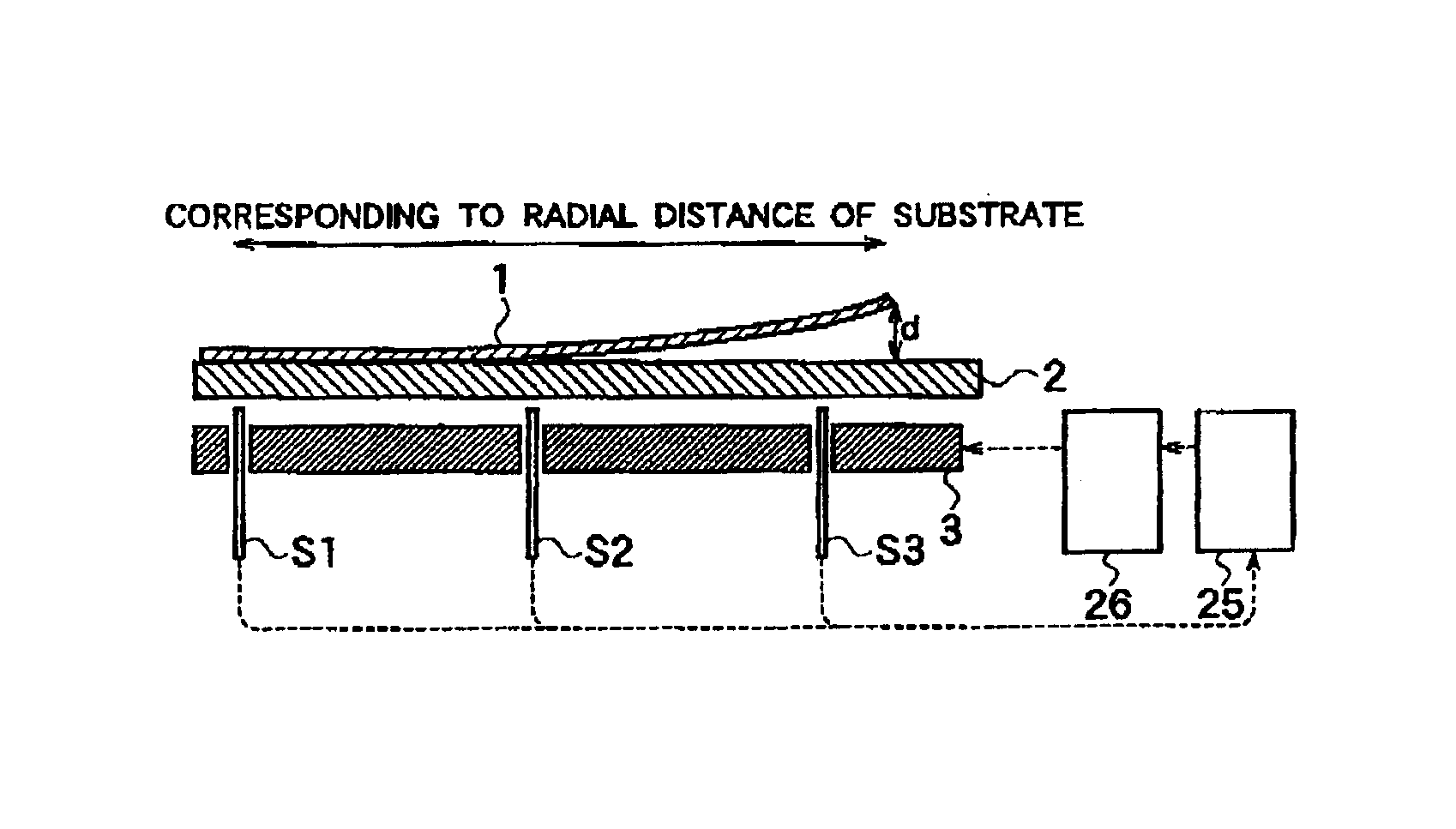
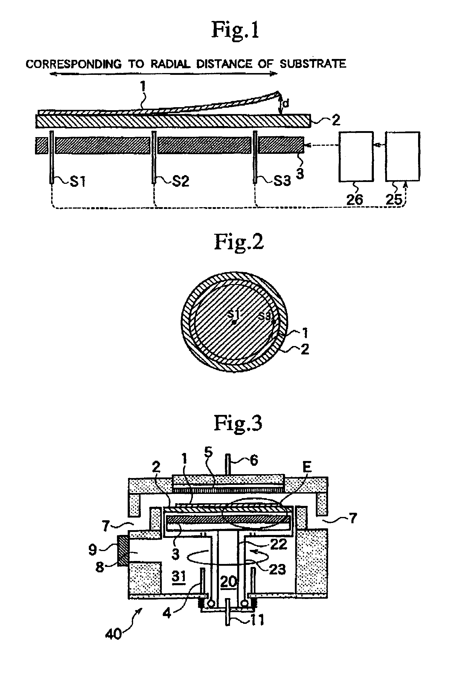
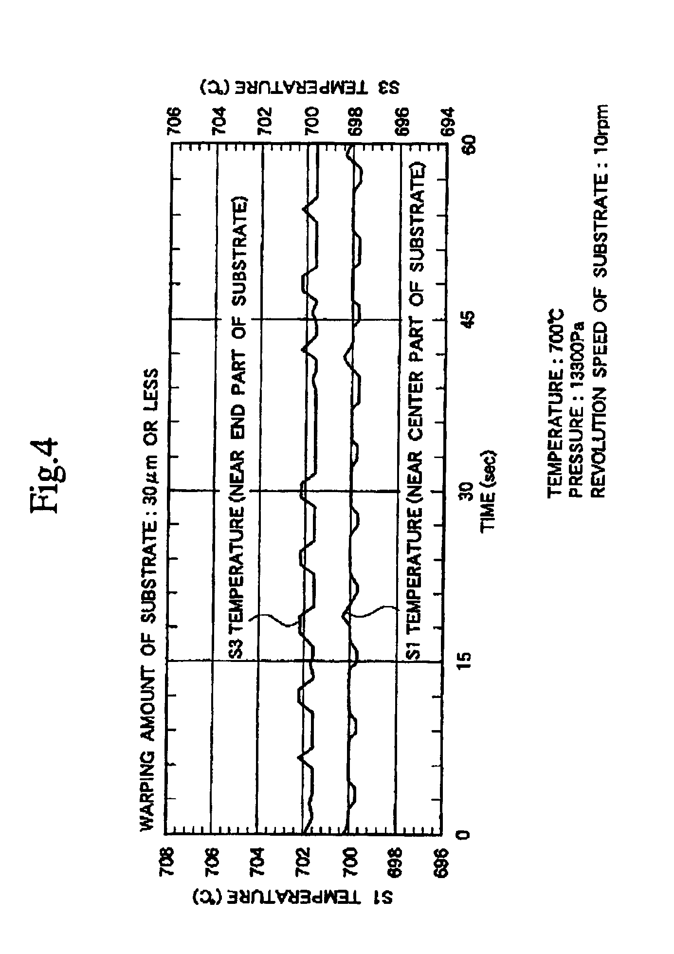
Hereinafter, explanations about embodiments of the present invention which are applied to a sheet-type substrate processing apparatus will be given. It should be noted that, although an apparatus of a single wafer type which performs processing for each substrate will be explained as the sheet type, it is not limited to the single wafer type and the embodiments of the present invention may be applied to an apparatus which performs processing of about two to five or more substrates.

FIG. 12 and FIG. 13 are schematic sectional views of the sheet-type substrate processing apparatus which performs thin film formation and heat treatment and is the premise of the embodiments.

The apparatus includes a hermetically structured processing container 40. The processing container 40 includes a substrate inserting port 8 through which a semiconductor substrate 1 such as a silicon wafer is carried from a carrying chamber (not shown) into a processing chamber 31 inside the processing container 40, an...


PUM

PropertyMeasurementUnit
temperatureaaaaaaaaaa
pressureaaaaaaaaaa
pressureaaaaaaaaaa

Abstract

By indirectly monitoring a warping amount of a substrate, it is possible to examine causes easily when substrate processing such as deposition is performed with nonuniform in-plane temperature of the substrate and a defect in a substrate characteristic, for example in uniformity of a film thickness, is caused. In a substrate processing apparatus for processing a substrate, a substrate holding body for holding the substrate on its surface and a resistance heater for heating the substrate through the substrate holding body are provided. Radiation thermometers for measuring temperature of the substrate holding body, which has a correlation with a warping amount of the substrate, from its rear surface side are provided to the resistance heater. The substrate holding body is provided to be rotatable with respect to the radiation thermometers so that temperature information of the substrate holding body in a circumferential direction can be obtained. A calculator as a monitor for monitoring the warping amount of the substrate having a correlation with the temperature of the substrate holding body, based on the measured values of the radiation thermometers, is provided. A command for correcting the warping amount is sent to a control means, based on the warping amount determined by the calculator, to control the resistance heater, as necessary.

Description

BACKGROUND OF THE INVENTION1. Field of the InventionThe present invention relates to a substrate processing apparatus and a method for manufacturing a semiconductor device and, more particularly, to those which monitor or control a warping amount of a substrate.2. Description of the Related ArtGenerally, in a sheet-type substrate processing apparatus, a substrate is processed while the substrate is forcedly sucked onto a substrate holding plate. In this case, when an adhesion of the substrate onto the substrate holding plate is not controlled, a problem is caused that a substrate characteristic of the substrate of the low adhesion is deteriorated seriously when it is transferred to a subsequent deposition process.Specifically, as shown in FIG. 14, the sheet-type substrate processing apparatus performs processing such as deposition on the substrate by spraying a gas in a shower state from a gas dispersing plate 5 which is disposed above a substrate 1, while the substrate 1 is sucked ...

Claims


Application Information

Patent Timeline
Patent Type & Authority Patents(United States)
IPC IPC(8): H01L21/66H05B3/00B05C9/14B05C11/08B05D1/40B05D3/00H01L21/205H01L21/683
CPCH01L22/26H01L22/00
Inventor TAKANO, SATOSHI
Owner KOKUSA ELECTRIC CO LTD
Why Eureka
Try Eureka