Thin-film transistor used as heating element for microreaction chamber

a technology of microreaction chamber and thin film transistor, which is applied in the direction of material heat development, laboratory glassware, instruments, etc., can solve the problems of limiting flexibility, ohmic resistors are subject to material degradation, electromigration, etc., and achieve the effect of easy etching or micromachining

Inactive Publication Date: 2005-03-08
STMICROELECTRONICS SRL
View PDF10 Cites 38 Cited by
  • Summary
  • Abstract
  • Description
  • Claims
  • Application Information

AI Technical Summary

Benefits of technology

The microreaction chamber is formed from a layer of material which can easily be etched or micromachined. For example, the microreaction chamber may be comprised of an o

Problems solved by technology

One drawback with this arrangement is that the resistance of such ohmic resistors is fixed and cannot be modulated, thus limiting their flexibility.
Other drawbacks are that ohmic resistors are subject to material degradation (such as oxidation, segregation,

Method used


Image

  • Thin-film transistor used as heating element for microreaction chamber
  • Thin-film transistor used as heating element for microreaction chamber
  • Thin-film transistor used as heating element for microreaction chamber

Examples


Embodiment Construction

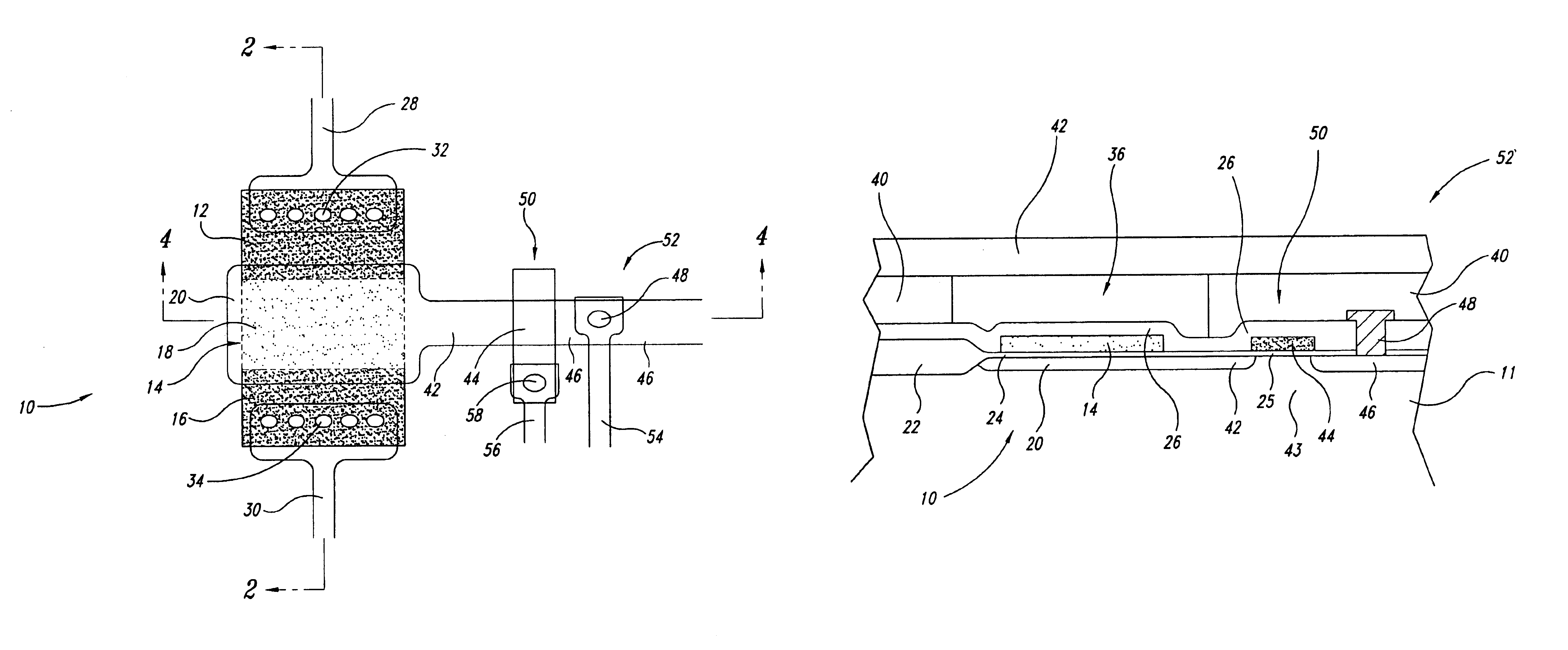
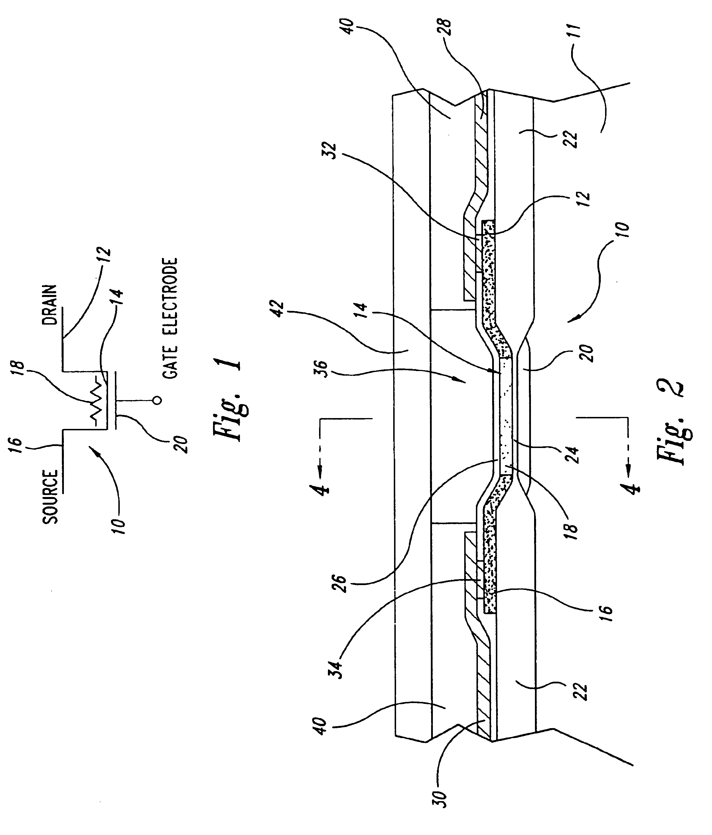
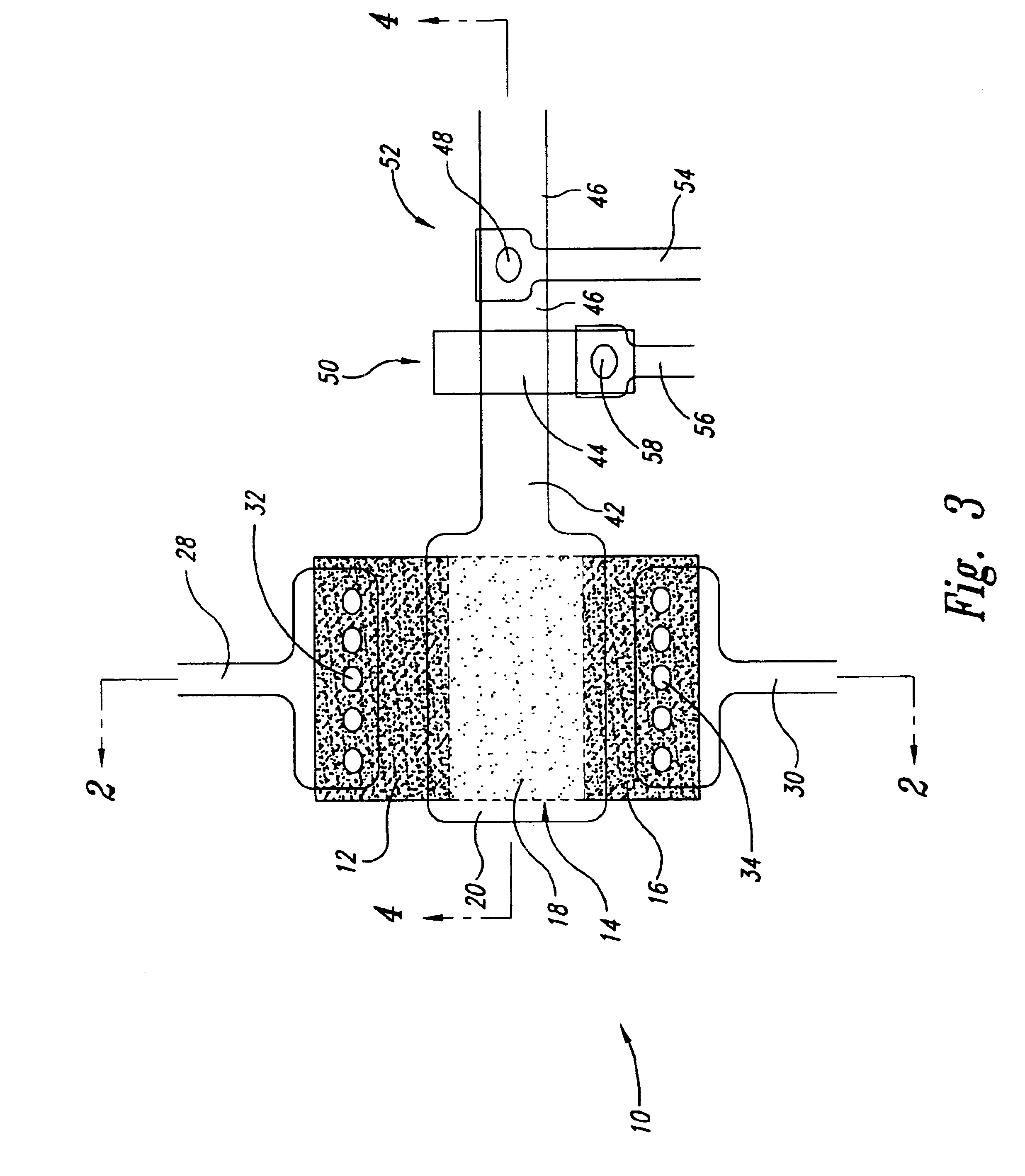
FIG. 1 is an electrical schematic of a thin-film transistor 10 which provides the heating element for a heater assembly according to principles of the present invention. The transistor 10 includes a drain region 12, a channel region 14, and a source region 16. Within the channel region 14 is a resistive element 18 which heats up in response to a current passing from the drain to the source. Adjacent the channel region 14 is a gate electrode 20. When a voltage is placed on the gate electrode 20, the transistor 10 is enabled so that a current may pass from the drain to the source via the channel region 14 and thus heat a resistive region within the channel region to a desired temperature.

FIG. 2 is a cross-sectional view of one embodiment of the thin-film transistor semiconductor heater assembly. A semiconductor substrate 11 is lightly doped having a desired conductivity type, and may be either a p-type or n-type depending on the desired configuration. Within the semiconductor region 1...


PUM


Abstract

The thin film transistor formed of polycrystalline silicon is positioned adjacent a heat reaction chamber. The gate electrode for the transistor is formed within a silicon substrate and a gate dielectric is positioned over the gate electrode. A pass transistor is coupled to the gate electrode, the pass transistor having a source/drain region in the same semiconductor substrate and positioned adjacent to the gate electrode of the thin film heating transistor. When the pass transistor is enabled, a voltage is applied to the gate electrode which causes the current to flow from the drain to the source of the thin film transistor. The current flow passes through a highly resistive region which generates heat that is transmitted to the heat reaction chamber.

Description

BACKGROUND OF THE INVENTION1. Field of the InventionThe present invention relates to a heater for a microreaction chamber and in particular, to use of a thin-film transistor as the heating element in the microreaction chamber and method of making the same.2. Description of the Related ArtThe treatment of some fluids, whether liquid or gas, involves an increasingly precise temperature regulation. It is frequently necessary to have very small amounts of fluid be rapidly elevated to a particular temperature under precise controls.Current inkjet technology relies on placing a small amount of ink within an ink chamber, rapidly heating the ink and ejecting it to provide an ink drop at a selected location on an adjacent surface, such as a sheet of paper. Traditionally, ohmic resistors which heat up rapidly when current is passed therethrough have been used to provide the necessary temperature increase of the ink. See, for example, a detailed discussion of ink ejection in an article titled ...

Claims


Application Information

Patent Timeline
IPC IPC(8): B01J19/00F24J3/00G01N25/20G01N25/48H01L29/786H01L21/02H01L21/336H01L29/66H01L37/00H05B3/22H05B3/26B01L3/00G01N35/00B41J2/05B41J2/16H05B3/00
CPCB01J19/0093B41J2/14129F24J3/00G01N25/4826H01L29/66765H01L29/78624H01L29/78696H05B3/26B01J2219/00828B01J2219/00853B01J2219/00873B01L3/5027G01N2035/00376H05B2203/013H05B2203/017B01J2219/00783F24V99/00
Inventor BRYANT, FRANK R.
Owner STMICROELECTRONICS SRL
Why Eureka
Try Eureka