Semiconductor device and method for fabricating the same

a semiconductor and device technology, applied in semiconductor devices, semiconductor/solid-state device details, electrical apparatus, etc., can solve the problems of narrow channel effect, insufficient reduction of parasitic capacitance cp, and inability to achieve narrow channel effect, and achieve small gate capacitance.

Inactive Publication Date: 2005-03-15
FUJITSU SEMICON LTD
View PDF12 Cites 11 Cited by
  • Summary
  • Abstract
  • Description
  • Claims
  • Application Information

AI Technical Summary

Benefits of technology

An object of the present invention is to provide a semiconductor device including a body contact, whose gate capacitance is small and which can suppress speed performance deterioration of the transistors, and a method for fabricating the semiconductor device.

Problems solved by technology

This floating body effect is a cause of device characteristic deviations, which makes margin design of a circuit difficult.
The reduction of the parasitic capacitance Cp is not enough.
Thus, a semiconductor device having body contact regions has excessive additions to a gate capacitance and a junction capacitance, and the effect of parasitic capacitance reduction, which is a merit of using SOI substrates cannot be sufficiently used.
STI technique is superior to the conventional LOCOS in micronization, but has the problem that the channel width dependency of the electric characteristics, especially sub-threshold characteristics of MOSFET becomes higher (narrow channel effect).
To solve this problem, the corners of the device region border are rounded, or etc. to thereby reduce the effect but insufficiently.

Method used


Image

  • Semiconductor device and method for fabricating the same
  • Semiconductor device and method for fabricating the same
  • Semiconductor device and method for fabricating the same

Examples


first embodiment

[A First Embodiment]

The semiconductor device according to a first embodiment of the present invention will be explained with reference to FIGS. 1, 2A-2C, 3, 4A-4B, 5A-5D, 6A-6C, 7A-7C, and 8A-8C.

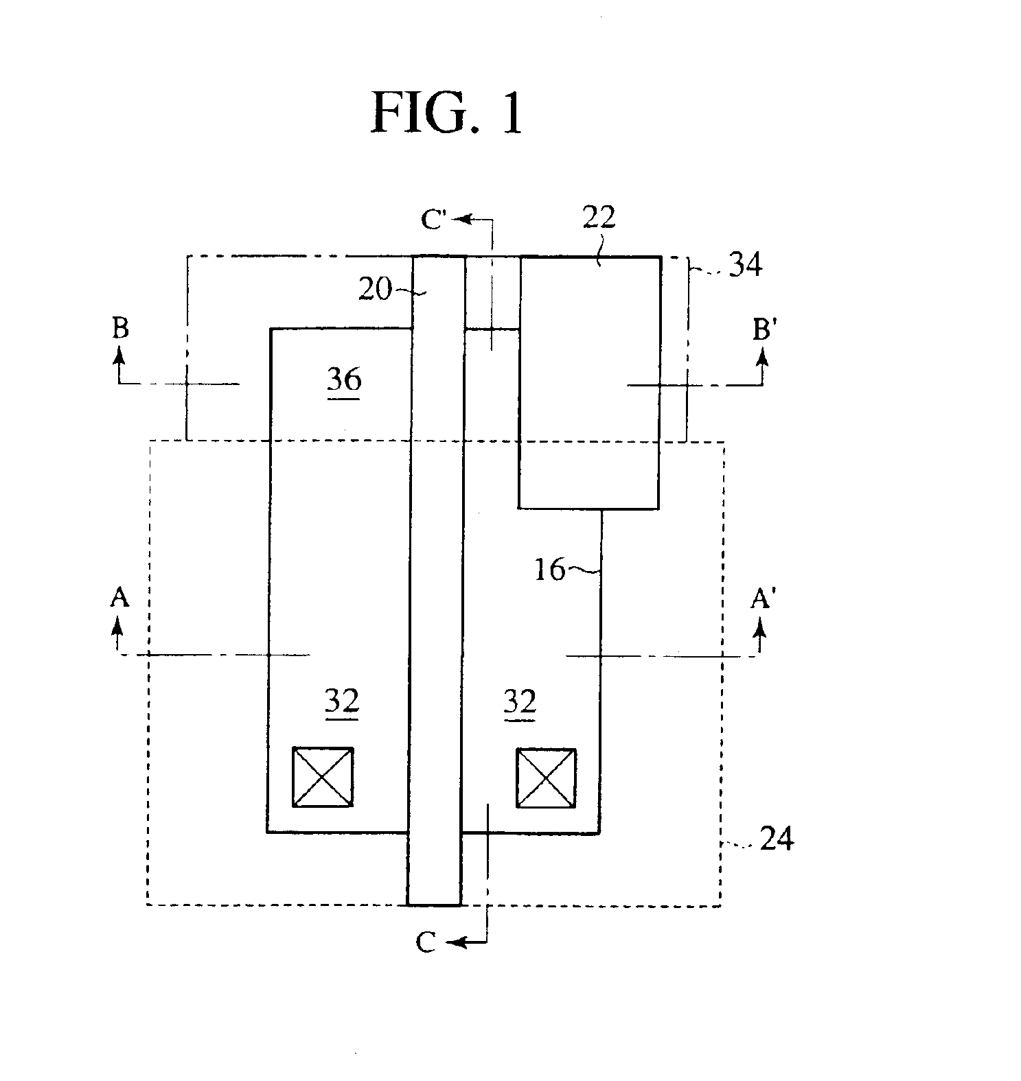
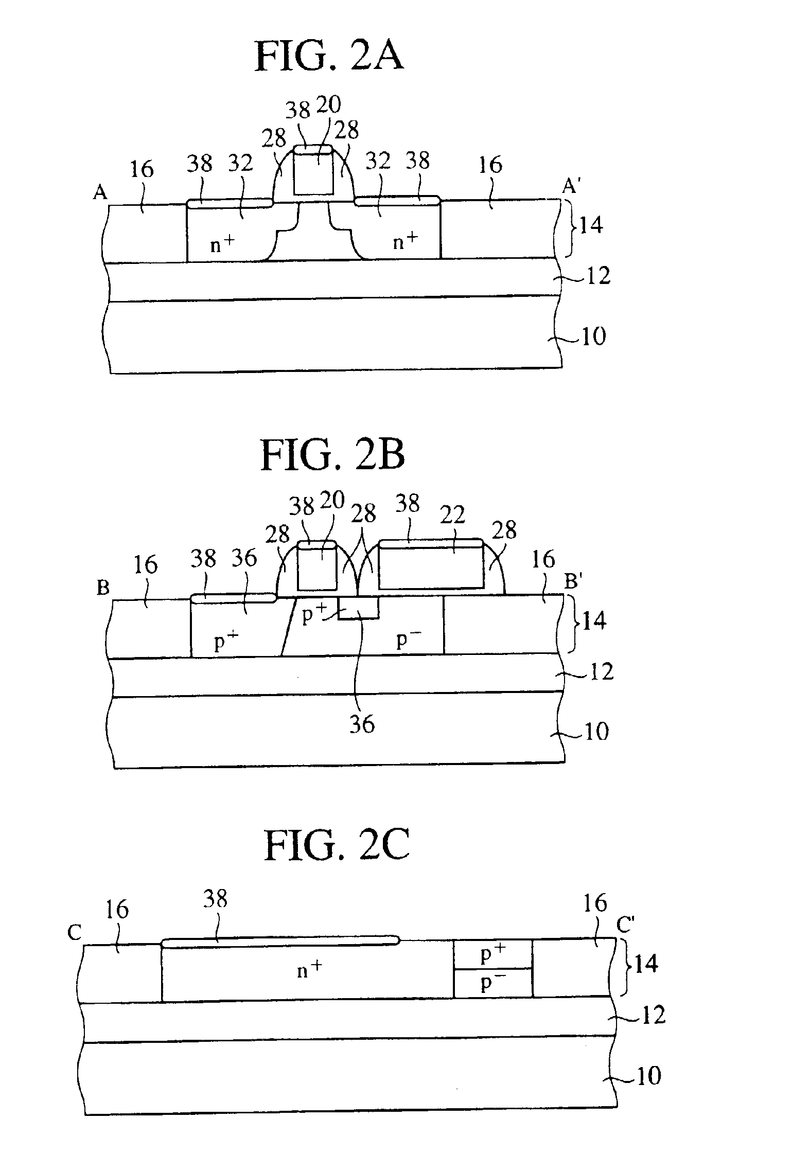
FIG. 1 is a plan view of the semiconductor device according to the present embodiment. FIGS. 2A-2C are diagrammatic sectional views of the semiconductor device according to the present embodiment, which show the structure thereof. FIG. 3 is a circuit diagram of an equivalent circuit of the semiconductor device according to the present embodiment. FIGS. 4A-4B are plan views of the semiconductor device according to the present embodiment and the conventional semiconductor device which show examples of parameters of the semiconductor device. FIGS. 5A-5D, 6A-6C, 7A-7C, and 8A-8C are sectional views of the semiconductor device according to the present embodiment in the steps of the method for fabricating the same, which explain the method.

First, the structure of the semiconductor device according...

second embodiment

[A Second Embodiment]

The semiconductor device and the method for fabricating the same according to a second embodiment of the present invention will be explained with reference to FIG. 9. The same members of the present embodiment as those of the semiconductor device and the method for fabricating the same according to the first embodiment are represented by the same reference numbers not to repeat or to simplify their explanation.

FIG. 9 is a plan view of the semiconductor device according to the present embodiment, which shows a structure thereof.

The semiconductor device and the method for fabricating the same according to the present embodiment are basically the same as the semiconductor device and the method for fabricating the same according to the first embodiment of the present invention. The semiconductor device according to the present embodiment is characterized in that two transistors are formed with one drain region in common in one device region and with one dummy electr...

third embodiment

[A Third Embodiment]

The semiconductor device and the method for fabricating the same according to a third embodiment of the present invention will be explained with reference to FIGS. 10A and 10B. The same members of the present embodiment as those of the semiconductor device and the method for fabricating the same according to the first and the second embodiments are represented by the same reference numbers not to repeat or to simplify their explanation.

FIG. 10A is a plan view of the semiconductor device according to the present embodiment. FIG. 10B is a diagrammatic sectional view of the semiconductor device according to the present invention along the line A-A′ in FIG. 10A.

The semiconductor device and the method for fabricating the same according to the present embodiment are the same as the semiconductor device and the method for fabricating the same according to the first embodiment except that a gate electrode 20 and a dummy electrode 22 have a positional relationship which i...


PUM


Abstract

The semiconductor device comprises: a conducting layer including: a channel region; a source region and a drain region sandwiching the channel region; and a body region connected to the channel region and being adjacent to the source region and the drain region; a gate electrode formed above the channel region interposing a gate insulation film therebetween; a dummy electrode formed on the body region near the interface between at least the drain region and the body region, and electrically insulated with the gate electrode; and a body contact region formed in the body region except a region where the dummy electrode is formed. The gate electrode and the dummy electrode are electrically insulated with each other, whereby the semiconductor device having body contacts can have a gate capacitance much decreased. Accordingly, deterioration of the speed performance of the transistors can be suppressed.

Description

BACKGROUND OF THE INVENTIONThe present invention relates to a semiconductor device having body contacts and a method for fabricating the semiconductor device, more specifically to a semiconductor device which has a reduced gate capacitance and suppresses speed performance deterioration of the transistors, and a method for fabricating the semiconductor device.Recently, as semiconductor devices are larger-scaled and more integrated, semiconductor integrated circuits are made to have higher performances and lower electric power consumption. It is proposed to use SOI (Silicon On Insulator) substrates. The SOI substrate is a substrate having a thin semiconductor layer formed on an insulation layer. The SOI substrate, which permits a device isolation film arriving at the insulation layer to fully isolate devices from each other, and also permits a dopant diffused layer formed in regions arriving at the insulation layer to much reduce junction leak current and junction capacitances. Thus, ...

Claims


Application Information

Patent Timeline
Patent Type & Authority Patents(United States)
IPC IPC(8): H01L29/786H01L29/417H01L29/423H01L29/45H01L29/66H01L29/40H01L21/3205H01L23/52H01L29/78
CPCH01L29/41733H01L29/42384H01L29/458H01L29/78615H01L29/78621H01L29/78645H01L29/78648H01L2924/0002H01L2924/00
Inventor YAMAGUCHI, SEIICHIROKAI, MITSUAKIAMANO, ISAO
Owner FUJITSU SEMICON LTD
Why Eureka
Try Eureka