

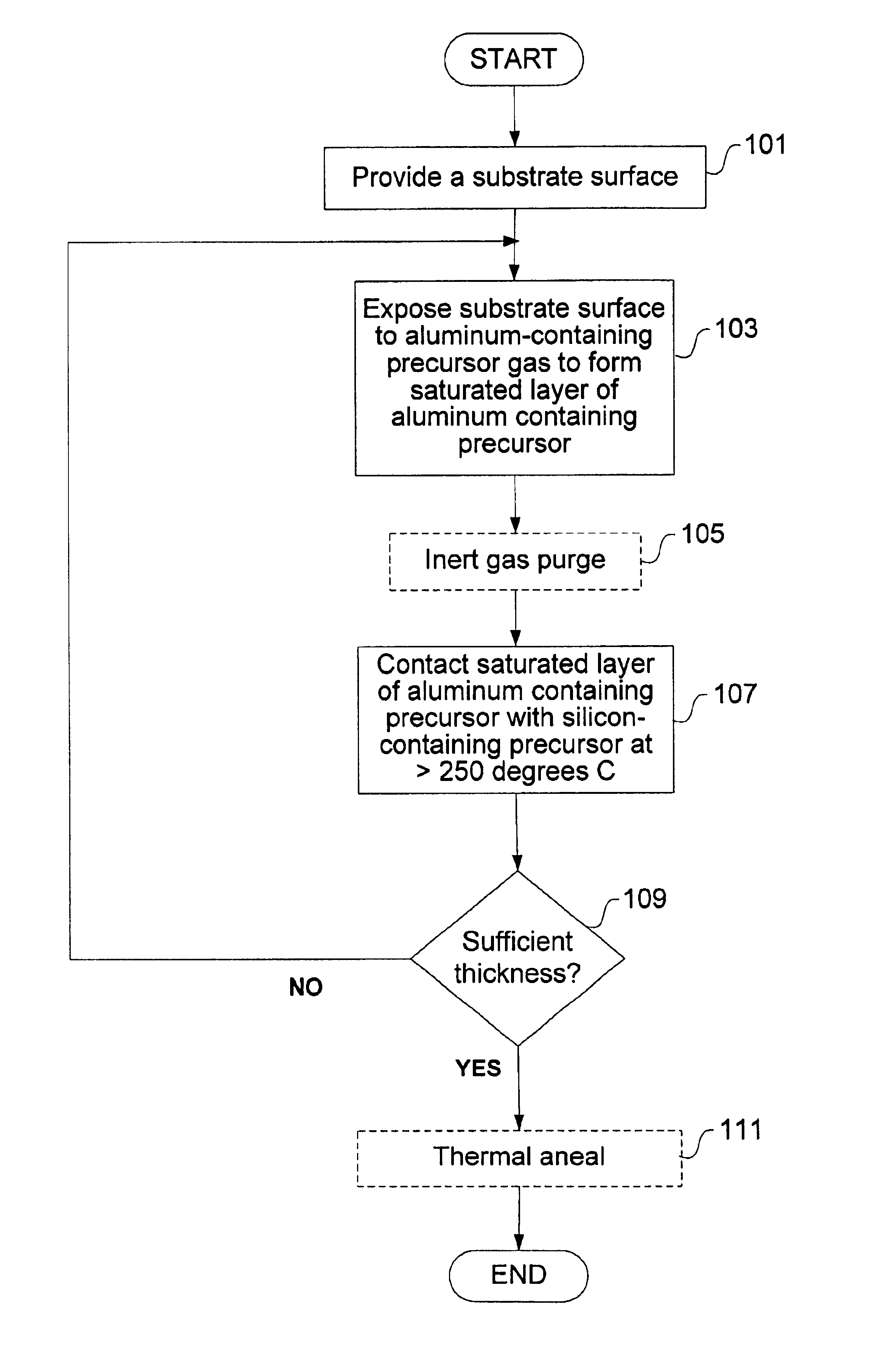
Properties of a silica thin film produced by a rapid vapor deposition (RVD) process
a technology of rapid vapor deposition and thin film, which is applied in the direction of chemical vapor deposition coating, coating, semiconductor devices, etc., can solve the problems of increasing the depth to width of sti features, low deposition rate, and insufficient conformal films of high aspect ratio features
- Summary
- Abstract
- Description
- Claims
- Application Information
AI Technical Summary
Benefits of technology
Problems solved by technology
Method used
Image

Examples
example 1
Film 1 and Film 2 were deposited using the following procedures.
[0046]A. Film 1 was deposited using a substrate temperature of about 200 degrees Celsius.
[0047]B. Film 2 was deposited using a substrate temperature of about 300 degrees Celsius.
[0048]C. Film 1 was further treated with a thermal anneal (1 hour at about 600 degrees Celsius).
[0049]D. Film 2 was further treated with a thermal anneal (1 hour at about 600 degrees Celsius).
[0050]After procedure A, Film 1 is measured and found to have k of about 6.9, a wet etch rate ratio (WERR) of about 6.7 and a post-anneal shrinkage percentage of about 6.1%. As stated previously, k refers to the dielectric constant of the film. A typical thermally grown silicon dioxide film has k of about 4. Water has a k of about 80. The WERR is the ratio of the rate in which the film can be etched relative to thermally grown silicon dioxide, which has a nominally low wet etch rate. Thus the WERR is reflected as (etch rate of the film) / (etch rate of therma...
example 2
[0053]Five films (A, B, C, D and E) were deposited using different deposition temperatures between 200 and 300 degrees Celsius. The film properties of these samples were then measured. Results are summarized in the following table.
Post 600CAnnealDepo-AverageDi-PostFilmsitionGrowthelectric600CStressTemp-RateCon-Wet etchAnneal(compres-erature(nm / stantrate ratioFilmsive)Film(C)cycle)(k)(WERR)Shrinkage(Gdyne / cm2)A20014.77.546.416.35%1.02B23015.66.475.836.02%0.98C25013.36.115.375.48%0.64D2758.65.774.003.57%0.08E3004.15.013.06%
[0054]As reflected by the forgoing results, k, WERR and the post-anneal shrinkage percentage all decrease as the deposition temperature increases. For example, Film A, which was deposited at 200° C., has a k of 7.54, a WERR of 6.41 and a post-anneal shrinkage percentage of 6.35% while Film E, which was deposited at 300° C., has a k of 5.01, a WER of less than 4 and a post-anneal shrinkage percentage of 3.06%. These results are consistent with the results of Example ...
PUM
| Property | Measurement | Unit |
|---|---|---|
| Temperature | aaaaa | aaaaa |
| Temperature | aaaaa | aaaaa |
| Temperature | aaaaa | aaaaa |
Abstract
Description
Claims
Application Information