

Method of power distribution analysis for I/O circuits in ASIC designs
- Summary
- Abstract
- Description
- Claims
- Application Information
AI Technical Summary
Benefits of technology
Problems solved by technology
Method used
Image

Examples
Embodiment Construction
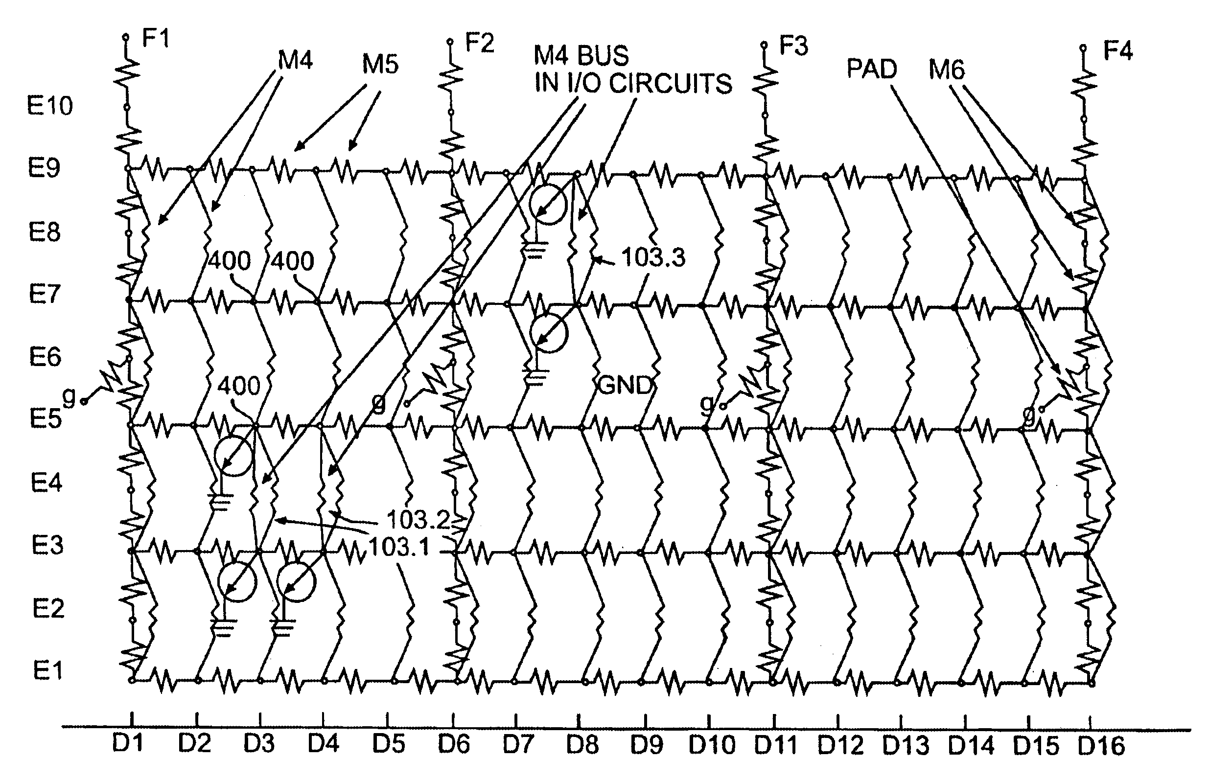
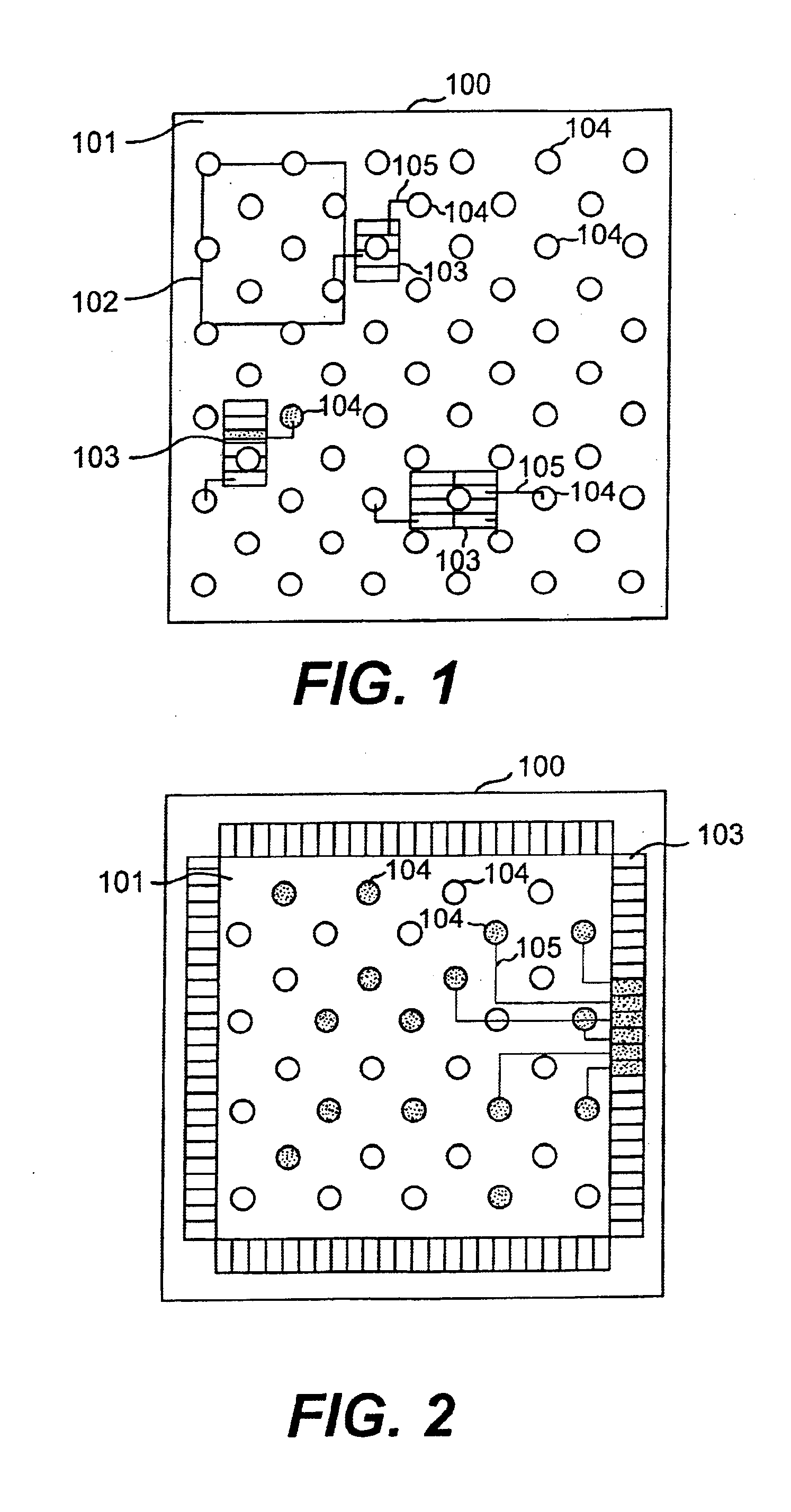
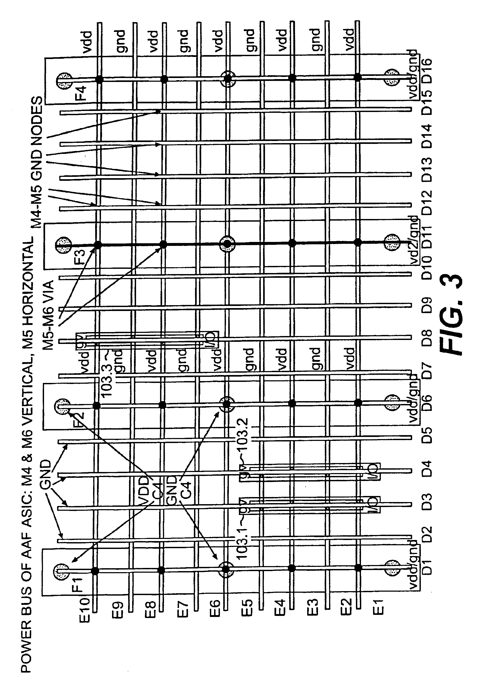
FIGS. 1 and 2 show examples of types of ASIC chip layouts to which the method according to the present invention may be advantageously applied. FIG. 1 shows an example of an area-array type chip layout. A chip 100 includes a logic area 101 containing logic circuits. The chip may also contain macros 102, which are pre-defined areas of logic already placed and routed.
Multiple chip layers are illustrated in the same plane in FIG. 1. The logic circuits and macros would typically reside on a lower layer. I / O circuits 103 for carrying signals on and off the chip may be distributed across the logic area, anywhere within snap grids defined for the I / O circuits. The snap grids are typically aligned with the major horizontal and vertical power buses of the power distribution network for the chip. A routed connection 105 may exist between an I / O circuit 103 and an I / O pad 104. The I / O pads 104 typically occupy an upper metal layer of the chip. The routed connection 105 is made between routing ...
PUM
 Abstract
Description
Claims
Application Information