Apparatus for manufacturing laminated member

a technology for laminated parts and apparatuses, applied in the direction of manufacturing tools, soldering apparatus, auxiliary welding devices, etc., can solve the problems of reducing the accuracy of positional alignment, reducing the size of manufacturing devices, and reducing the productivity of manufacturing devices, so as to achieve the effect of increasing the closeness

Inactive Publication Date: 2005-03-22
UHT CORP
View PDF13 Cites 18 Cited by
  • Summary
  • Abstract
  • Description
  • Claims
  • Application Information

AI Technical Summary

Benefits of technology

In addition, it is preferable to press the upper surface of the thin film layer at a proper time such as every time one thin film layer is formed so as to keep the uniform flatness from the fine corrugations generated at the ceramics slurry, insulating resin paste, conductive paste of the thin film layer, make a uniform laminated layer and increase an accuracy of lamination. In order to attain this effect, the temporary press contacting means comprised of a heating plate or a roll and the like are added to and arranged side by side against the segment path where the base plate is moved (7th aspect).
If any one of the aforesaid inventions were provided with a pressing means for pressing upper surfaces of the insulating sheets at a proper time when the insulating sheets are overlapped to each other, the upper surface of the insulating sheet might be made flat due to the fact that the upper surface of the insulating sheet is pressed by the pressing means, thereby an accuracy in lamination of subsequent thin film layer could be increased, a close fitness between the insulating sheet and the thin film layer could be increased to cause each of the layers to be uniformly integrated and at the same time a high quality laminated member could be attained.

Problems solved by technology

However, in accordance with this prior art manufacturing method, after the thin film layers formed on a carrier film are peeled off by every one layer, they are laminated, so that it becomes necessary to arrange both a peeling mechanism and a laminating mechanism not only to cause a manufacturing device to become large in size but also to reduce its productivity, and it shows a problem in accuracy in positional alignment due to the fact that the thin film layers once peeled off are laminated.
However, even in the case that the metallic endless belt is used in place of the base plate, this system provides some inconveniences that it needs a large mounting floor area to cause the device to become large in size and its facility expenditure is increased in the same manner as found in the aforesaid prior art in reference to the number of arrangement of the slurry injection heads or the paste injection heads, addition of drying means for drying an insulation layer and an electrode layer, a temporary pressing means or a main pressing means for increasing a productivity and the recovering segment for the formed laminated member.
In addition, both ceramics slurry and the functional material paste were injected in a repetitive manner through the slurry injection head and the paste injection head above the base plates moving in both X-axis and Y-axis directions to form a laminated member, so that it was difficult to assure a flatness at each of the layers.
That is, the aforesaid prior art had a problem that a flatness of the surface became a deteriorated state due to a formation of some fine corrugations at the surface of a thin film layer formed under injection of either the ceramics slurry or functional material paste, and also showed a certain problem in an inner accuracy of the completed laminated member.
Additionally, the prior art also had a problem that an injection work took much time due to the fact that the flat ceramics layer was formed by injecting ceramics slurry.
In addition, when a layer composed of some inner circuit elements is formed on the ceramics layer to form one thin film layer, a notch fitting segment is produced between the electrode layers at a layer composed of the inner circuit elements to deteriorate a flatness of the thin film layer, resulting in that when the thin film layers are laminated, a clearance is generated by the notch fitting segment and it may become a cause of generating a void in the electronic parts after baking operation.

Method used


Image

  • Apparatus for manufacturing laminated member
  • Apparatus for manufacturing laminated member
  • Apparatus for manufacturing laminated member

Examples


Embodiment Construction

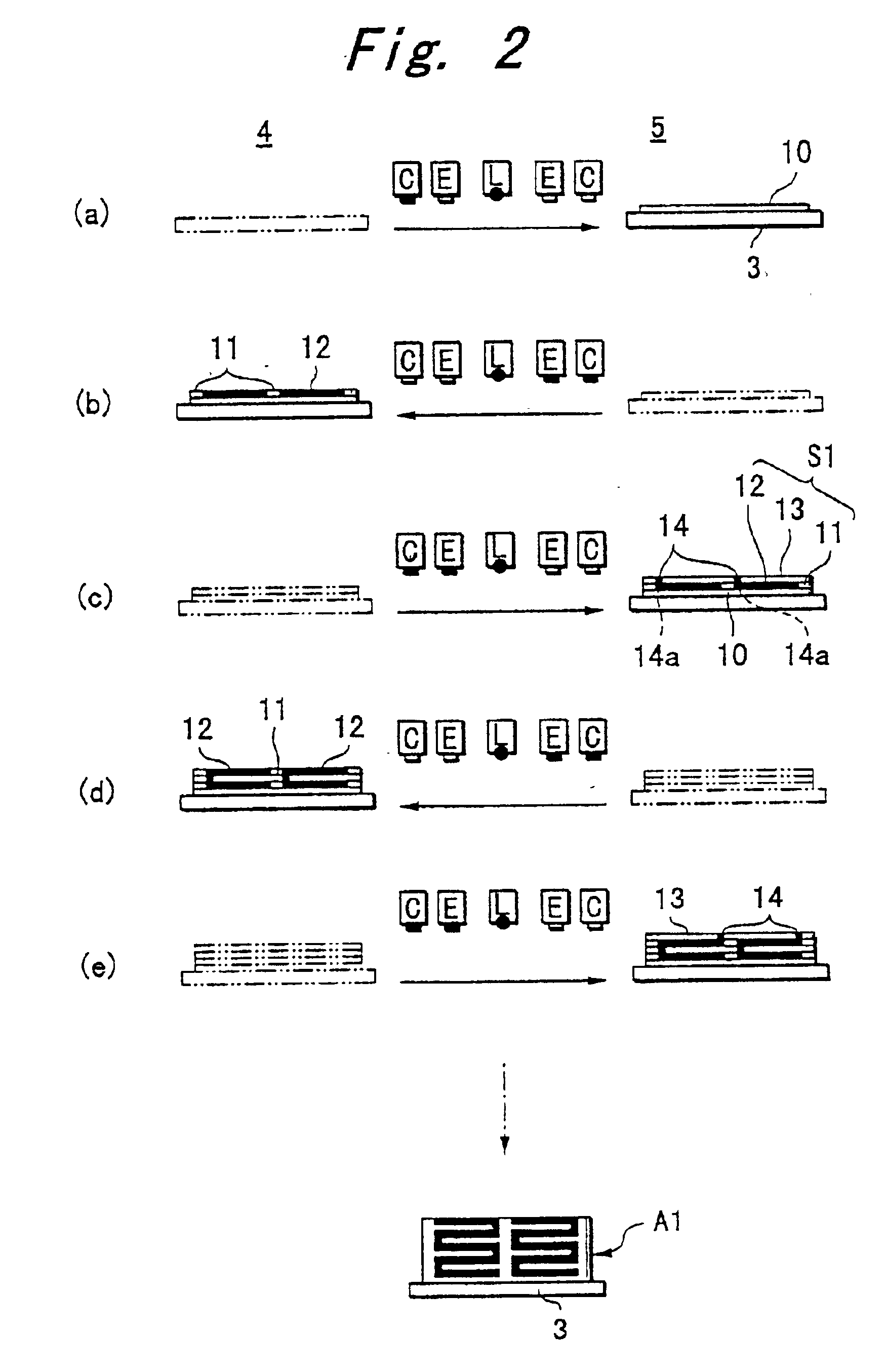
Referring now to the drawings, some preferred embodiments of the present invention will be described as follows.

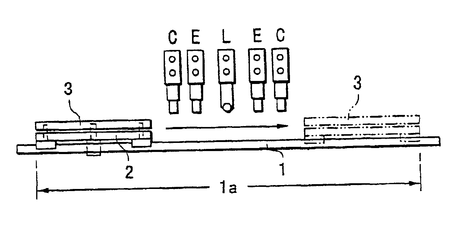
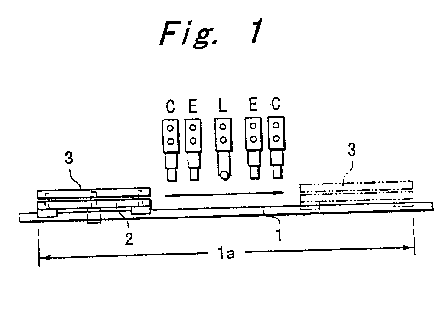
Then, some preferred embodiments of the present invention will be described as follows, wherein in the case of the present preferred embodiments, the laminated type capacitor and laminated type inductor of the laminated type electronic component parts are described.

That is, the preferred embodiments illustrate a manufacturing apparatus for manufacturing the laminated capacitor and laminated inductor by coating ceramics slurry through the insulating layer forming means, arranging the electrode pattern on the insulating layer through the conductive layer forming means to form the thin film layer and repeating these operation.

A first invention of the apparatus for manufacturing the laminated member shown in FIGS. 1 to 17 will be described as follows, wherein FIG. 1 schematically shows a manufacturing apparatus that is installed within a machine frame not shown, wherein a mova...


PUM

PropertyMeasurementUnit
lengthaaaaaaaaaa
thicknessaaaaaaaaaa
widthaaaaaaaaaa

Abstract

A manufacturing speed for a laminated member for every layer is increased to improve productivity and at the same time a small-sized manufacturing apparatus capable of being practically realized is provided. A base plate is mounted at a linear predetermined segment path in such a way that it can be reciprocated and moved up and down, each of one to a plurality of an insulating layer forming means for discharging ceramics slurry or insulating resin paste, conductive layer forming means for injecting conductive paste by an ink jet system and drying means for drying said slurry, paste are arranged side by side on the segment path, the thin film layer having a predetermined electrode pattern arranged thereon is formed on the ceramics insulating layer while the base plate reciprocates by once to several times over the segment path, and these operations are repeated to form the laminated member.

Description

BACKGROUND OF THE INVENTION1. Field of the InventionThis invention relates to an apparatus for manufacturing a laminated member, and more particularly an apparatus for manufacturing some laminated electronic component parts such as a capacitor, an inductor or a resistor, a magnetic member and a filter or the like installed on the laminated substrate.2. Description of the Related ArtAs a usual method for manufacturing a typical ceramics laminated member of laminated members, it is well known in the art to provide some steps of coating ceramics slurry by a doctor blade process onto a carrier film composed of a long polyethylene terephthalate or the like; drying it; then printing a conductive paste onto the upper surface of dried slurry by a screen printing process; drying it to form a ceramics thin film layer; thereafter peeling off the thin film layer from the carrier film; cutting it into a predetermined shape in reference to a position of its inner electrode pattern; and laminating...

Claims


Application Information

Patent Timeline
Patent Type & Authority Patents(United States)
IPC IPC(8): B32B37/24B32B37/14H05K3/46H05K3/12H01F41/04H01G4/30
CPCB32B37/24H05K3/4664H01G4/30B32B2037/243B32B2315/02B32B2457/16Y10T156/1798H05K3/1241Y10T156/1304
Inventor KAKIMOTO, MASAKAZUMATSUMOTO, FUMIAKIYASODA, HISASHIFURUTA, MAKOTO
Owner UHT CORP
Why Eureka
Try Eureka