Exposure method and method of manufacturing semiconductor device

a semiconductor and exposure method technology, applied in the field of exposure method and exposure method of manufacturing a semiconductor device, can solve the problems of affecting the size of a circuit pattern, the inability to obtain the desired pattern, and the influence of aberration of the projection lens in the exposure apparatus, so as to achieve the effect of higher light intensities

Inactive Publication Date: 2005-03-29
KK TOSHIBA
View PDF15 Cites 0 Cited by
  • Summary
  • Abstract
  • Description
  • Claims
  • Application Information

AI Technical Summary

Benefits of technology

By adjusting the positional relationship between the illumination system and the projection lens in this manner, the influence of 3θ aberration can be suppressed. This makes it possible to correct the asymmetry of the light intensity distribution on the wafer due to 3θ aberration and greatly reduce variations in pattern size on the wafer.

Problems solved by technology

Recently, with a reduction in the size of a circuit pattern, the influence of aberration of a projection lens in an exposure apparatus poses a problem.
As a consequence, an asymmetrical pattern is projected on the wafer, and no desired pattern can be obtained.
With regard to 3θ aberration, it is very difficult to perform lens adjustment.
It is therefore very difficult to solve the problem that the asymmetrical pattern is projected on a wafer.
For this reason, the problem that the asymmetrical pattern is projected on a wafer becomes more serious.
As described above, with a reduction in the size of a circuit pattern, it becomes more difficult to obtain a desired pattern because of the influence of the aberration of a projection lens.
It is especially difficult to reduce the influence of 3θ aberration.

Method used


Image

  • Exposure method and method of manufacturing semiconductor device
  • Exposure method and method of manufacturing semiconductor device
  • Exposure method and method of manufacturing semiconductor device

Examples


first embodiment

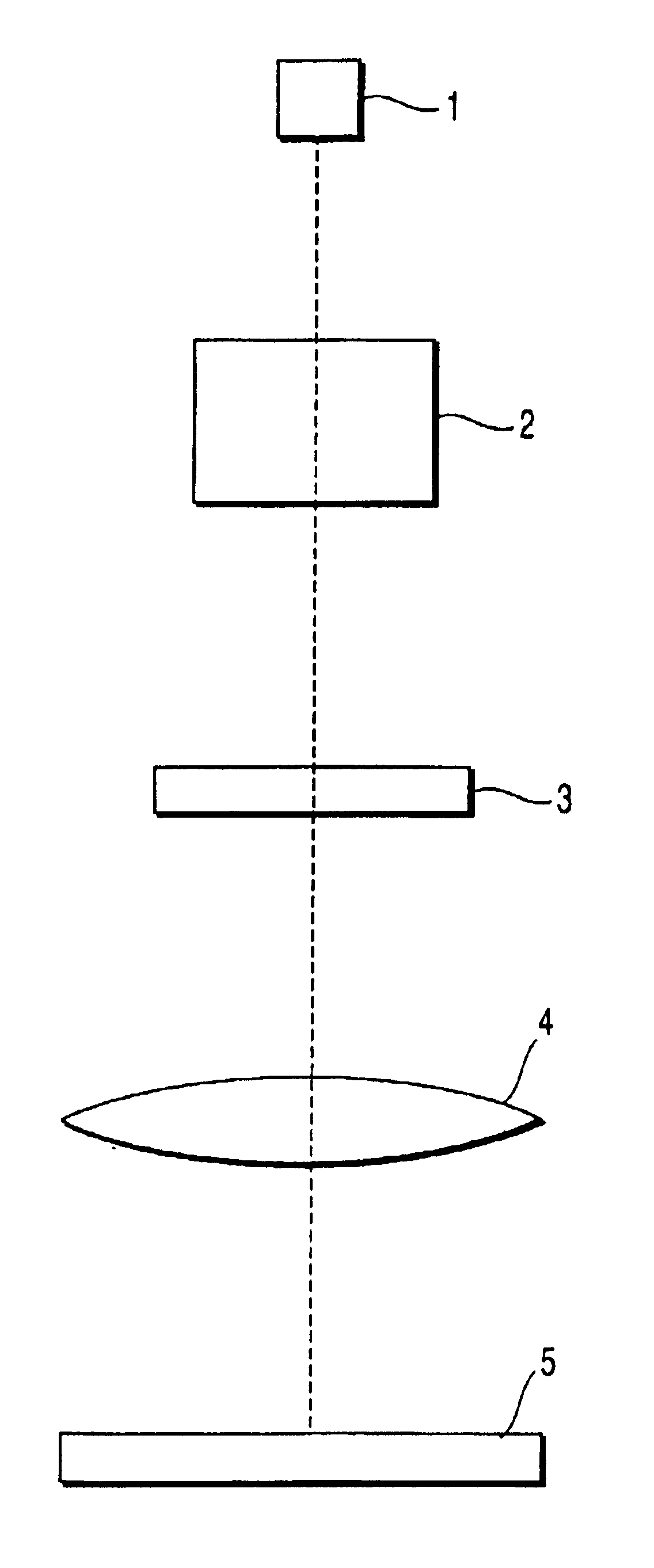
FIG. 1 is a view showing the schematic arrangement of an exposure apparatus according to the first embodiment of the present invention.

This apparatus is basically the same as a general exposure apparatus. After a photomask (reticle) 3 having a desired mask pattern is set in the exposure apparatus, the photomask 3 having the desired mask pattern is irradiated with illumination light from an illumination system including a light source 1 and illumination optical system 2. A pattern image formed by the light that has passed through the photomask (reticle) 3 is projected on a resist on a wafer (semiconductor substrate) 5 through a projection lens (projection optical system) 4. In this case, if the projection optical system includes a plurality of lenses, the projection lens 4 means such a set of lenses, and is assumed to be a lens having optical characteristics equivalent to those obtained by such lenses.

A comparative example of this embodiment will be described with reference to FIGS. ...

second embodiment

The second embodiment of the present invention will be described next. The arrangement of an exposure apparatus is the same as that in the first embodiment shown in FIG. 1.

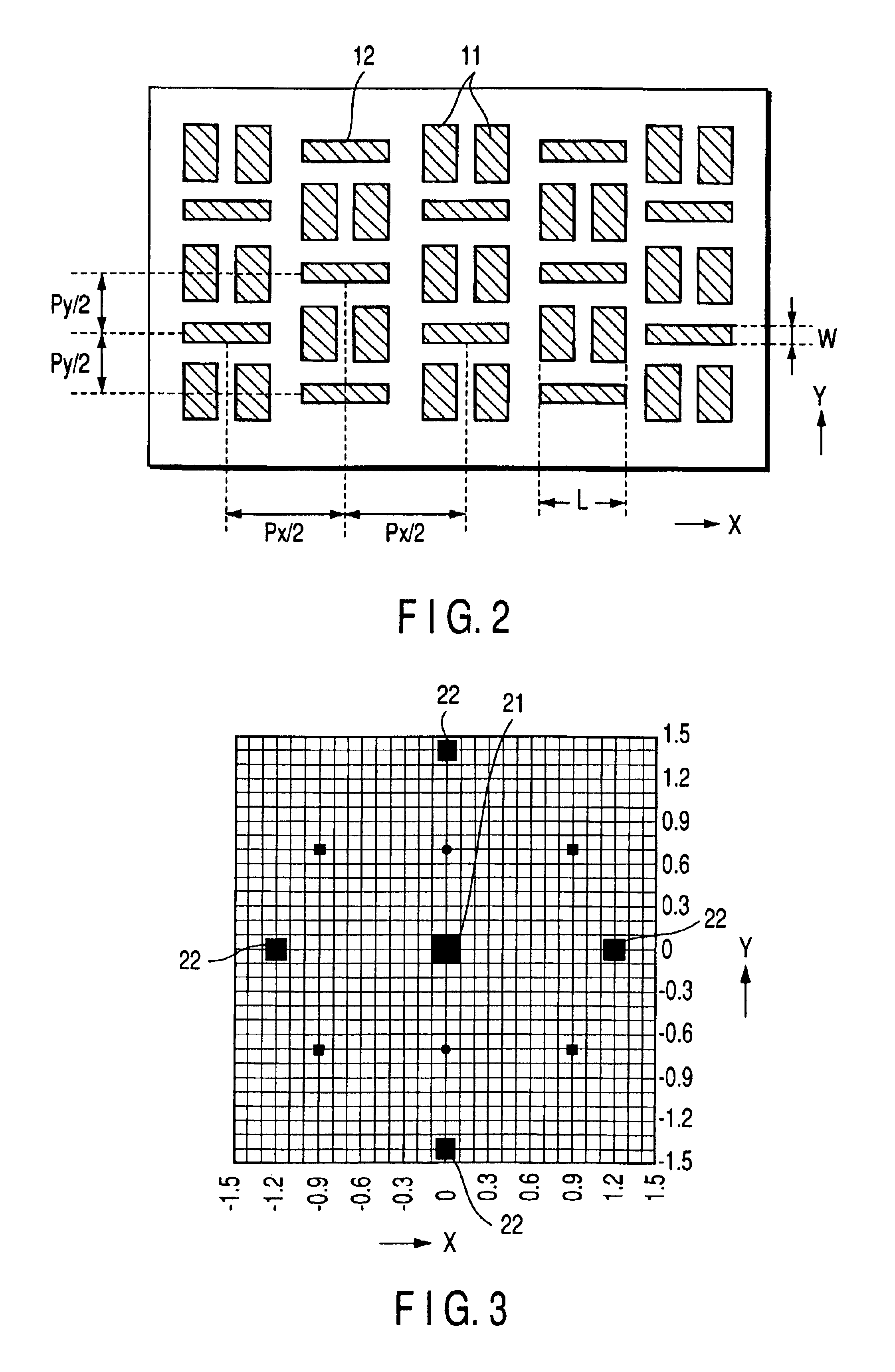
FIG. 6 shows a mask pattern formed on a photomask 3 in a comparative example of this embodiment. The mask pattern includes a plurality of unit circuit patterns 13 arranged in the checkered flag pattern. The respective unit circuit patterns 13 are arranged in the X and Y directions in predetermined cycles. The cycle in the X direction is represented by Px; and the cycle in the Y direction, Py. Each unit circuit pattern 13 is a so-called line pattern for wiring, which is widely used in semiconductor integrated circuits, and has a rectangular shape whose longitudinal direction coincides with the X direction.

In practice, each unit circuit pattern 13 has a complicated polygonal shape that has undergone optical proximity correction. As in the first embodiment, for the sake of simplicity, FIG. 6 shows the unit circuit pa...

third embodiment

FIG. 8 is a view showing the schematic arrangement of an exposure apparatus according to the third embodiment of the present invention.

The basic arrangement of the exposure apparatus shown in FIG. 8 is the same as that of the exposure apparatus shown in FIG. 1. In addition to the constituent elements shown in FIG. 1, the exposure apparatus of this embodiment includes an adjustment system (adjustment mechanism) 6 for adjusting the relative angle defined by an illumination system including a light source 1 and an illumination optical system 2 and a projection lens 4 in the rotational direction (circumferential direction of the projection lens 4). The illumination system has a light shielding area, and hence an illumination shape having the light shielding area can be obtained.

When the pattern shown in FIG. 4 in the first embodiment or the pattern shown in FIG. 6 in the second embodiment is used as a pattern on a photomask 3, the influence of 3θ aberration of the projection lens 4 is s...


PUM

PropertyMeasurementUnit
light intensitiesaaaaaaaaaa
widthaaaaaaaaaa
lengthaaaaaaaaaa

Abstract

Disclosed is an exposure method comprising preparing an exposure apparatus including an illumination system and a projection lens, setting, in the exposure apparatus, a photomask having a mask pattern including a plurality of unit circuit patterns arranged like a checkered flag pattern and a plurality of unit auxiliary patterns arranged between the unit circuit patterns, and projecting the mask pattern onto a substrate through the projection lens by irradiating the photomask with light from the illumination system, wherein the unit circuit patterns and the unit auxiliary patterns generate a plurality of diffraction light spots on a pupil plane of the projection lens, and the four diffraction light spots having higher light intensities than the remaining diffraction light spots are distributed on the pupil plane in a cycle of 90°.

Description

CROSS-REFERENCE TO RELATED APPLICATIONSThis application is based upon and claims the benefit of priority from the prior Japanese Patent Application No. 2001-195165, filed Jun. 27, 2001, the entire contents of which are incorporated herein by reference.BACKGROUND OF THE INVENTION1. Field of the InventionThe present invention relates to an exposure method and a method of manufacturing a semiconductor device and, more particularly, to a technique of reducing the influence of aberration in a lithography process.2. Description of the Related ArtRecently, with a reduction in the size of a circuit pattern, the influence of aberration of a projection lens in an exposure apparatus poses a problem.As the aberration of the projection lens decreases, optophysical treatment is required. For this reason, the aberration of an optical system is converted into wave aberration. As a method of expressing wave aberration as a function of pupil coordinate, a method using the Zernike polynomial is widely...

Claims


Application Information

Patent Timeline
Patent Type & Authority Patents(United States)
IPC IPC(8): G03F7/20G02B5/18G03F1/36G03F1/70H01L21/027H01L21/301
CPCG03F7/70433H01L21/027
Inventor KOMINE, NOBUHIROASANUMA, KEITAHIGASHIKI, TATSUHIKO
Owner KK TOSHIBA
Why Eureka
Try Eureka