Solid state image sensor and method for fabricating the same

a solid-state image sensor and fabricating method technology, applied in the direction of transistors, television systems, radio control devices, etc., can solve the problems of micro lens dissolution, deformation or detachment, and difficulty in applying a cmos circuit fabricating process without modification, so as to minimize dissolution, deformation and detachment

Inactive Publication Date: 2005-03-29
NEC ELECTRONICS CORP
View PDF7 Cites 48 Cited by
  • Summary
  • Abstract
  • Description
  • Claims
  • Application Information

AI Technical Summary

Benefits of technology

Another object of the present invention is to provide a structure and a fabricating method of a solid state

Problems solved by technology

In addition, since the CCD type solid state image sensor is fabricated with an inherent fabricating process, it is difficult to apply a CMOS circuit fabricating process with no modification.
In this first prior art example of the solid state image sensor as shown in FIG. 4B, however, the interface state that was reduced by the sintering

Method used


Image

  • Solid state image sensor and method for fabricating the same
  • Solid state image sensor and method for fabricating the same
  • Solid state image sensor and method for fabricating the same

Examples


first embodiment

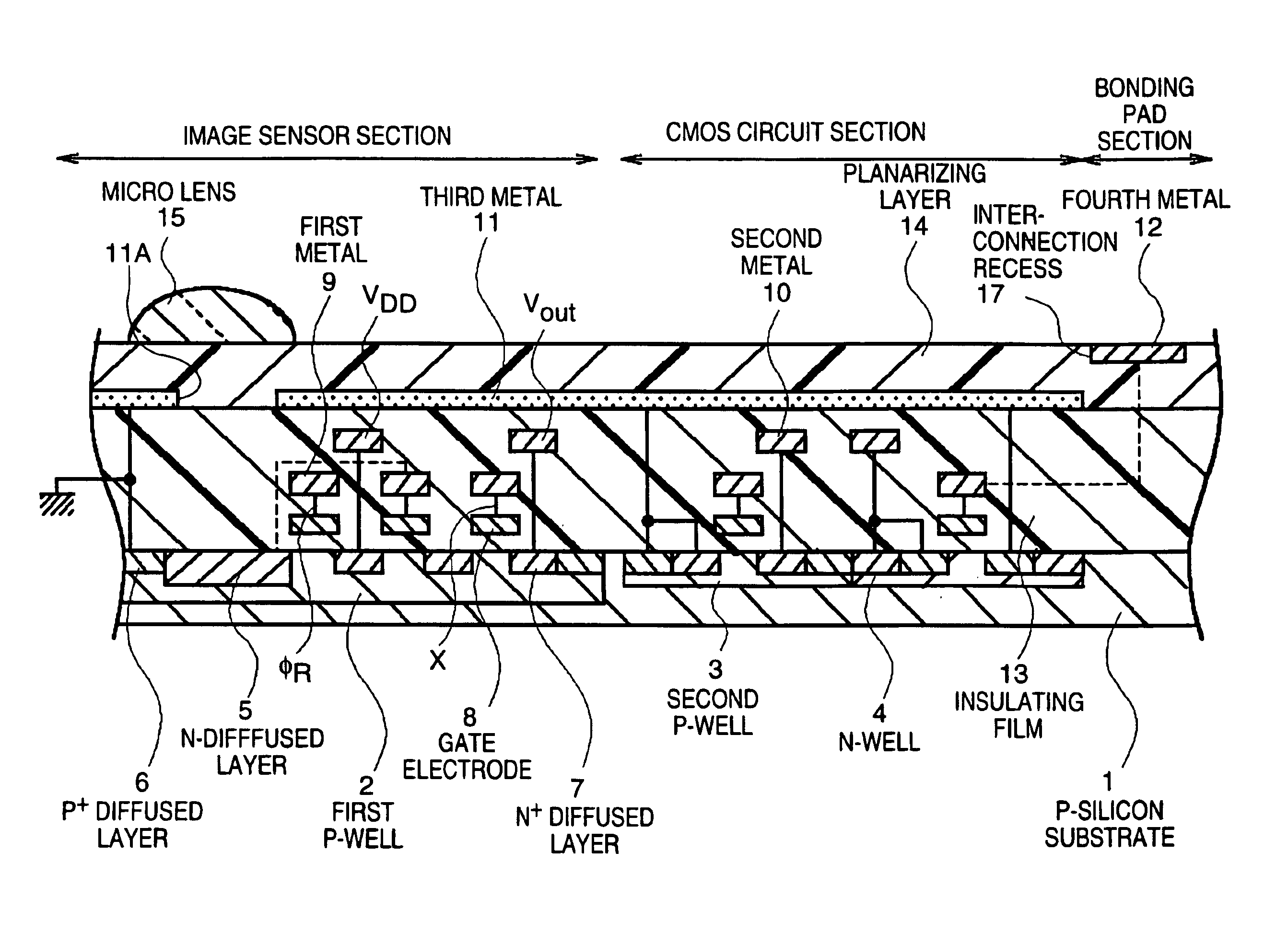
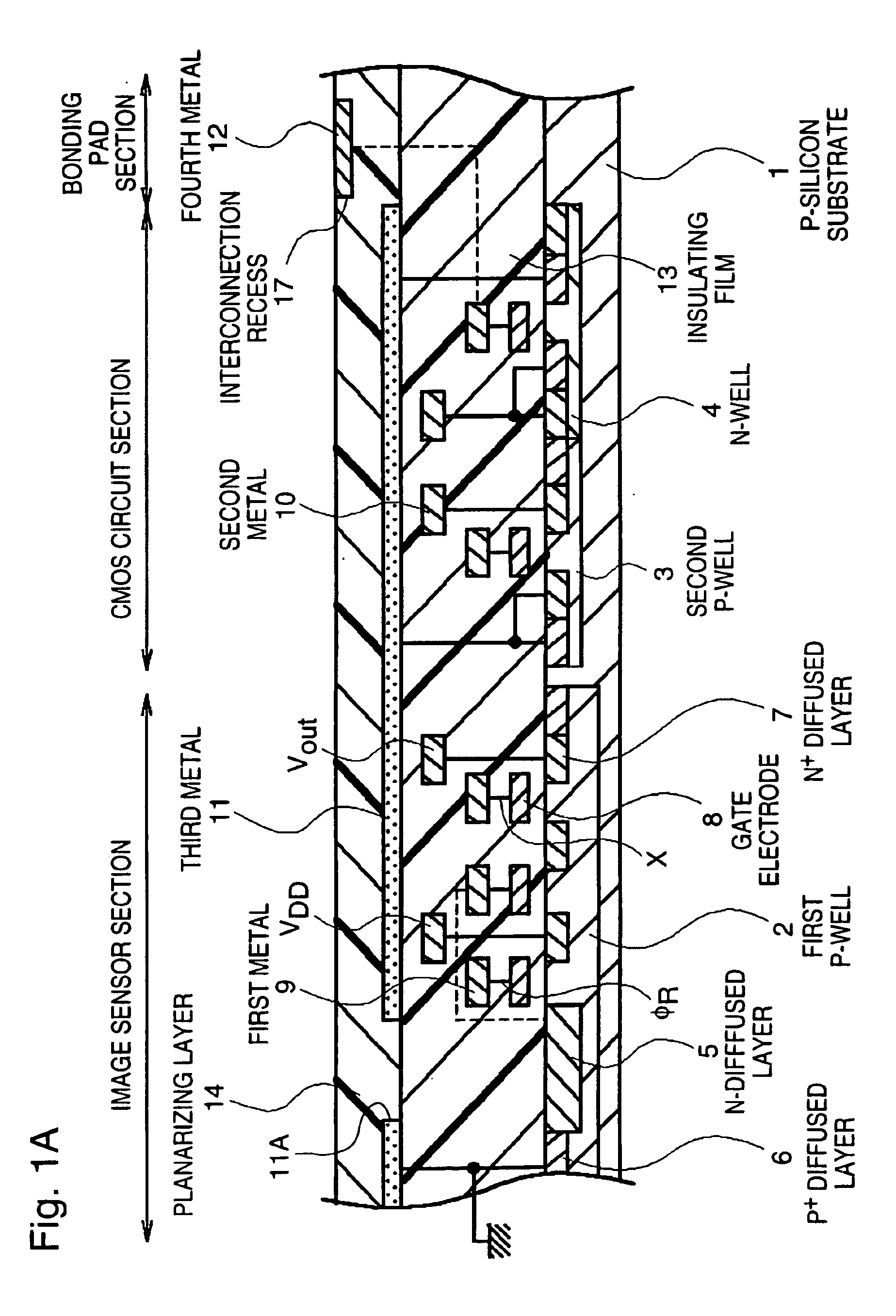
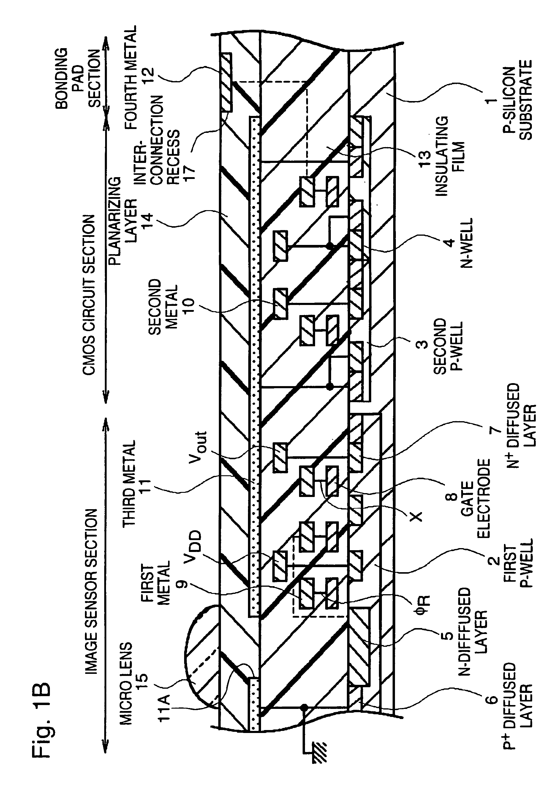
Referring to FIGS. 1A and 1B, there are shown diagrammatic partial sectional views of the solid state image sensor for illustrating the method in accordance with the present invention for fabricating the solid state image sensor. In FIGS. 1A and 1B, elements corresponding to those shown in FIG. 3A are given the same reference numbers, and therefore, explanation will be omitted for simplification of the description.

The structure under an upper surface of the insulating film 13, which includes a protection film and interlayer insulator films for the gate electrode and the interconnection, is the same as that of the prior art example. After the insulating film 13 in the first prior art example shown in FIG. 3A is formed, a third metal interconnection 11 also functioning as a light blocking film having an opening 11A at a position corresponding to the N-type diffused layer 5, is formed on the upper surface of the insulating film 13. At this time, the bonding pad is not formed, different...


PUM


Abstract

In a solid state image sensor having micro lenses, the micro lens and a bonding pad electrode are formed on a planarizing layer. Thus, it is no longer necessary to etch the planarizing layer for exposing the bonding pad under the planarizing layer, by use of a photolithography, and therefore, it is possible to avoid dissolution, deform and detachment of the micro lens, which would have otherwise been caused in the prior art by dissolving a photoresist which was used in the photolithography.

Description

BACKGROUND OF THE INVENTIONThe present invention relates to a structure and a fabricating method of a solid state image sensor having micro lenses.A conventional solid state image sensor of the type having a transfer layer for transferring a signal charge obtained by a photo-electric conversion, is generally classified into a MOS type and a CCD type. This solid state image sensor, particularly the CCD type solid state image sensor is recently widely used in a single-unit video-camera recorder, a digital camera, a facsimile, etc., and, at present, technology development is still continuously attempted for elevating the characteristics.The CCD type solid state image sensor includes a photoelectric conversion section, namely, an image sensor section, which is constituted by arranging in a two-dimensional array a number of photoelectric conversion elements corresponding to pixels. Signal charges obtained in the photoelectric conversion section are read out in order through a vertically ...

Claims


Application Information

Patent Timeline
IPC IPC(8): H01L27/146H01L27/14H04N5/335H04N5/369H04N5/374
CPCH01L27/14601H01L27/14623H01L27/14685H01L27/14634H01L27/14636H01L27/14627H01L27/146
Inventor NAKASHIBA, YASUTAKA
Owner NEC ELECTRONICS CORP
Why Eureka
Try Eureka