
Semiconductor device and manufacturing method thereof

a technology of semiconductor devices and manufacturing methods, applied in semiconductor devices, semiconductor/solid-state device details, electrical apparatus, etc., can solve problems such as achieve the effects of suppressing pad peeling increasing the area of the top surface or the bottom surface of improving the adhesion between the bonding pad portion and the insulating film

Active Publication Date: 2005-03-29
SEIKO EPSON CORP
View PDF1 Cites 2 Cited by
  • Summary
  • Abstract
  • Description
  • Claims
  • Application Information

AI Technical Summary

Benefits of technology

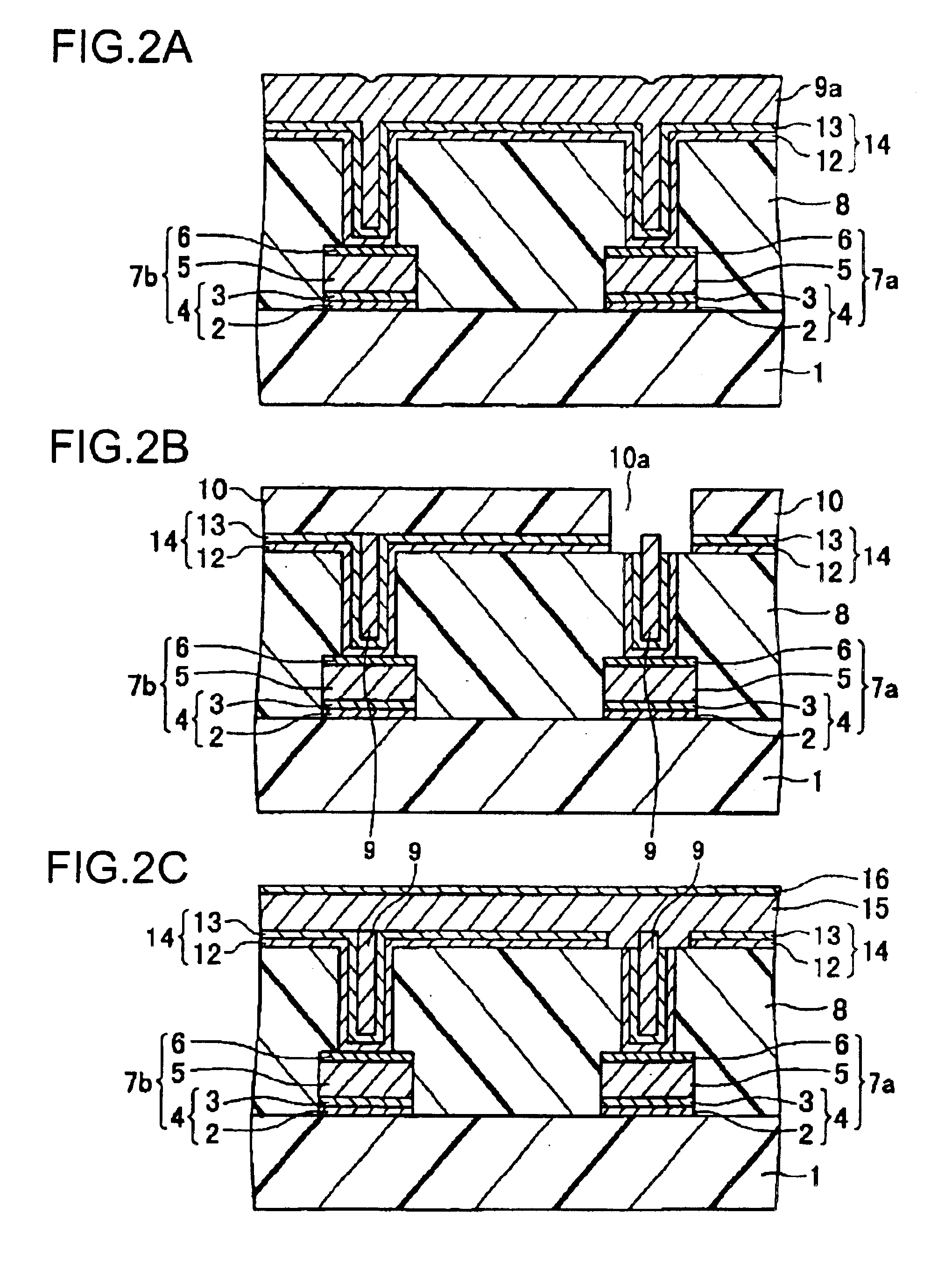
According to the method for manufacturing a semiconductor device, described above, in the removing step of removing at least a part of the barrier metal layer located under the position at which the pad opening portion is to be formed, the barrier metal layer is removed that is located under the position described above and on the insulating film. Accordingly, at the position at which the barrier metal layer is removed, the formation of a vulnerable alloy layer having poor stress resistance at the interface between the barrier metal layer and the insulating film can be suppressed. Hence, when a wire is bonded to the bonding pad portion by bonding connection, even if a stress caused by this bonding connection is applied to the bonding pad portion, the peeling thereof caused by this stress can be suppressed.
According to the method for manufacturing a semiconductor device, described above, in the removing step of removing at least a part of the barrier metal layer located under the position at which the pad opening portion is to be formed, the barrier metal layer is removed that is located under the position described above and on the insulating film. Accordingly, at the position at which the barrier metal layer is removed, the formation of a vulnerable alloy layer having poor stress resistance at the interface between the barrier metal layer and the insulating film can be suppressed. Hence, the peeling of the bonding pad portion caused by this stress can be suppressed.
According to the method for manufacturing a semiconductor device, described above, since the sidewall is formed on the inside surface of the connecting hole, the conductive film can be easily provided in the connecting hole due to the presence of this sidewall. Accordingly, the increase in connection resistance or the generation of connection failures can be suppressed in the connecting hole.
According to the method for manufacturing a semiconductor device, described above, since the pad opening portion is not formed over the metal plug, the area of the top surface or the bottom surface of the bonding pad portion can be increased. Hence, the adhesion between the bonding pad portion and the insulating film can be improved. As a result, when bonding connection is performed, pad peeling of the bonding pad portion can be suppressed.

Problems solved by technology

As a result, peeling of the bonding pad portion occurs.

Method used


Image

  • Semiconductor device and manufacturing method thereof
  • Semiconductor device and manufacturing method thereof
  • Semiconductor device and manufacturing method thereof

Examples


first embodiment

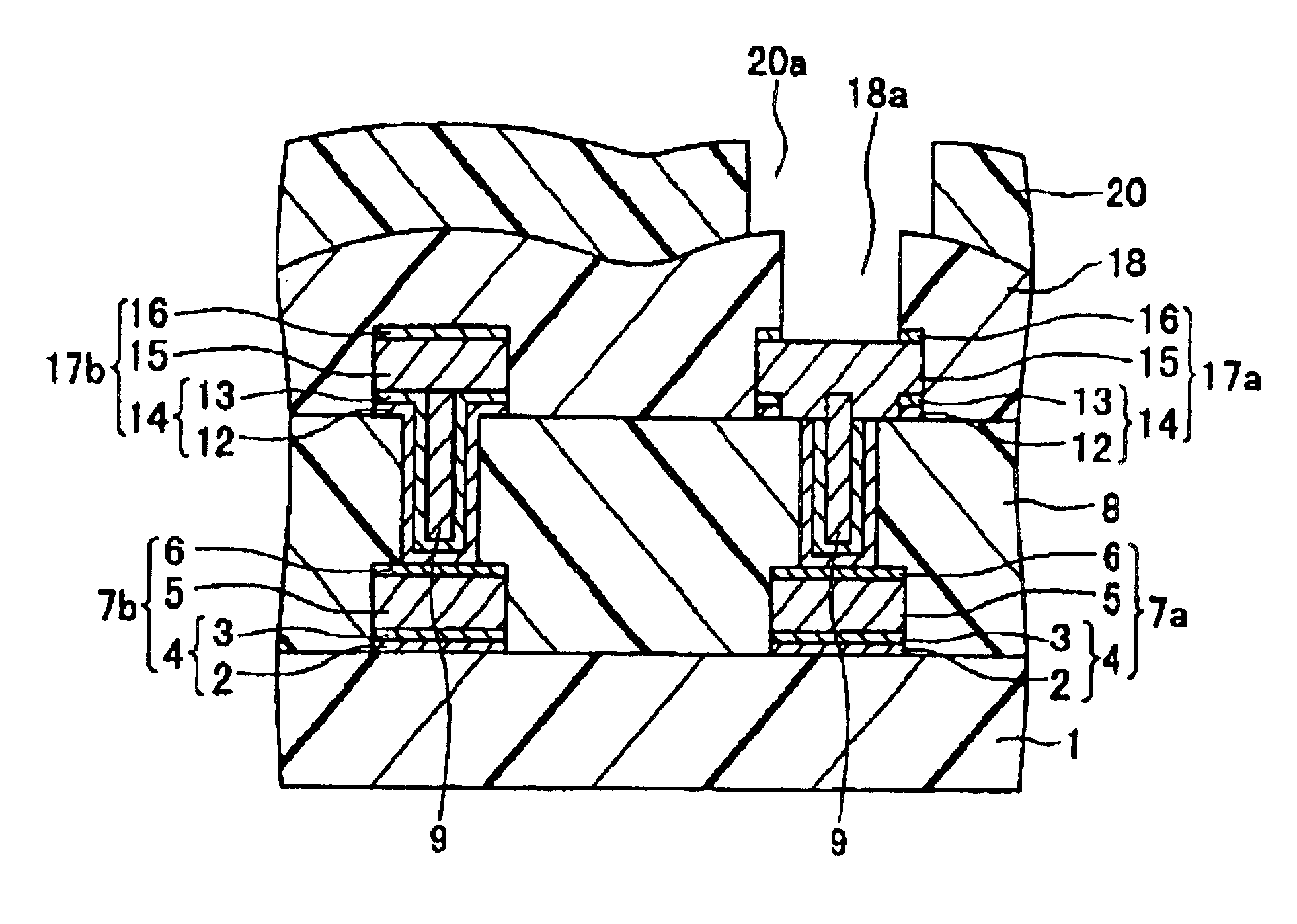
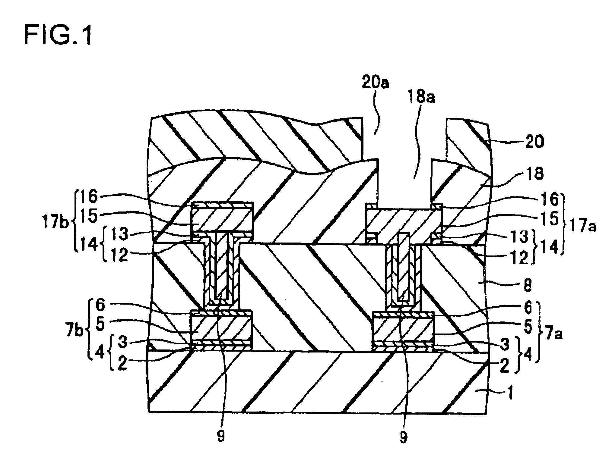
FIG. 1 is a cross-sectional view showing a semiconductor device of a first embodiment according to the present invention. This semiconductor device has bonding pad portions.

On an insulating film 1, first Al alloy wires 7a are 7b are formed. The first Al alloy wires 7a and 7b are each formed of a barrier metal layer 4, a first Al alloy film 5, and a antireflection film 6 provided in that order from the bottom. The barrier metal layer 4 is formed of a Ti film 2 and a TiN film 3 provided thereon.

On the first Al alloy wires 7a and 7b and the insulating film 1, an interlayer insulating film 8 containing Si is formed. In this interlayer insulating film 8, via holes (connecting holes) are formed at positions located on the first Al alloy wires 7a and 7b. Inside the connecting hole and on the interlayer insulating film 8, barrier metal layers 14 are formed. The barrier metal layer 14 is composed of a Ti film 12 and a TiN film 13 provided thereon.

On the barrier metal layer 14 provided in eac...

second embodiment

FIG. 4 is a cross-sectional view of a semiconductor device according to the present invention, the same reference numerals of the constituent elements described above designate the same constituent elements in this embodiment, and different constituent elements will only be described.

On the inside surface of the via hole (connecting hole) formed in the interlayer insulating film 8, a sidewall 21 made of a W film is formed with the barrier metal layer 14 provided therebetween.

The second Al alloy film (or a conductive film) 15 is formed on the side wall 21, inside the connecting hole, and on the barrier metal layer 14, and on the second Al alloy film 15, the antireflection film 16 is formed. The antireflection film 16, the second Al alloy film 15, and the barrier metal layer 14 form the bonding pad portion 17a.

That is, the bonding pad portion 17a is electrically connected to the first Al alloy wire 7a via the side wall 21 and the second Al alloy film 15 provided in the via hole.

A par...

third embodiment

FIG. 7 is a cross-sectional view of a semiconductor device according to the present invention. The same reference numerals of the constituent elements described above designate the same constituent elements in this embodiment, and different constituent elements will only be described.

On the W plug 9, the bonding pad portion 17a is formed. On the bonding pad portion 17a and the interlayer insulating film 8, the passivation film 18 is formed, and the opening portion 18a is formed in this passivation film 18 at a position located on the bonding pad portion 17a. The polyimide film 20 is formed on the passivation film 18, and the opening portion 20a is formed in this polyimide film 20. This opening portion 20a and the opening portion 18a described above form the pad opening portion. This pad opening portion is not located over the W plug 9 and is located at a position on the bonding pad portion 17a, which position is adjacent to the W plug 9 or in the vicinity thereof.

FIGS. 8(A) to (C) a...


PUM

PropertyMeasurementUnit
conductiveaaaaaaaaaa
insulatingaaaaaaaaaa
stressaaaaaaaaaa

Abstract

A method for manufacturing a semiconductor device is provided including: a step of forming a solid barrier metal layer on an interlayer insulating film; a removing step of removing at least a part of the solid barrier metal layer located at a place at which a pad opening portion is to be formed; a step of forming a solid second Al alloy film on the interlayer insulating film exposed in the removing step described above and the solid barrier metal layer; a step of patterning the solid second Al alloy film and the solid barrier metal layer so as to form a bonding pad portion on the interlayer insulating film; a step of forming a passivation film on the bonding pad portion and the interlayer insulating film; and a step of forming the pad opening portion in the passivation film at a position located on the bonding pad portion.

Description

RELATED APPLICATIONSThis application claims priority to Japanese Patent Application Nos. 2003-054002 filed Feb. 28, 2003 and 2004-023936 filed Jan. 30, 2004 which are hereby expressly incorporated by reference herein in their entireties.BACKGROUND1. Technical Field of the InventionThe present invention relates to semiconductor devices and manufacturing methods thereof, and more particularly, relates to a semiconductor device and a manufacturing method thereof, in which pad peeling of a bonding pad portion is suppressed.2. Description of the Related ArtFIG. 16 is a cross-sectional view showing a conventional semiconductor device. This semiconductor device has bonding pad portions.On a silicon substrate not shown in the figure, an insulating film 101 is formed, and on this insulating film 101, a Ti film 102 is deposited by sputtering, followed by deposition of a TiN film 103 thereon by sputtering. A barrier metal layer 104 made of the Ti film 102 and the TiN film 103 is formed on the ...

Claims


Application Information

Patent Timeline
Patent Type & Authority Patents(United States)
IPC IPC(8): H01L23/52H01L23/522H01L23/485H01L23/48H01L23/532H01L21/3205H01L21/60H01L21/768
CPCH01L21/76838H01L23/5226H01L23/53223H01L24/03H01L24/11H01L2924/01004H01L2224/0401H01L2924/01006H01L2924/01013H01L2924/01014H01L2924/01022H01L2924/0105H01L2924/01074H01L2924/04941H01L2924/05042H01L2224/13099H01L2924/01033H01L2224/45124H01L2924/01005H01L2224/02166H01L2924/00014H01L2924/00H01L2224/48
Inventor WADA, KOICHINAMATAME, TATSURU
Owner SEIKO EPSON CORP
Learn More