High precision orientation alignment and gap control stages for imprint lithography processes

a technology of imprint lithography and orientation alignment, which is applied in the field of small device manufacturing, can solve the problems of loss of overlay alignment registration, high undesirable, and prior art patents that do not disclose designs with the necessary high stiffness, and achieve the effect of reducing manufacturing cycles

Inactive Publication Date: 2005-03-29
BOARD OF RGT THE UNIV OF TEXAS SYST +1
View PDF163 Cites 473 Cited by
  • Summary
  • Abstract
  • Description
  • Claims
  • Application Information

AI Technical Summary

Benefits of technology

A technical advantage of the present invention is the achievement of imprint lithography without high temperatures or high pressures.
is the achievement of imprint lithography without high temperatures or high pressures.
Another technical advantage of the present invention is that separation of the template from the substrate is achieved without shearing of imprinted features.
Still another technical advantage of the invention is reduced manufacturing cycles since course alignment of the template is achieved once for each batch of die.

Problems solved by technology

Wafer motion in the x-y plane can cause loss of registration for overlay alignment.
The prior art patents do not, however, disclose designs with the necessary high stiffness to avoid lateral and twisting motions.
Such motion is highly undesirable in imprint lithography since it leads to unwanted overlay errors and could lead to shearing of fabricated structures.
The design shown in U.S. Pat. No. 4,355,469 is intended to accommodate larger lateral and rotational error than the designs shown in the first two patents, but this design does not have the capability to constraint undesirable lateral and twisting motions for imprint lithography.
The use of high temperatures and pressures, however, is undesirable in imprint lithography since they result in unwanted stresses being placed on the device.
Since the template and substrate are often made of different materials, expansion creates serious layer-to-layer alignment problems.
To avoid differences in expansion, the same material can be used but this limits material choices and increases overall costs of fabrication.
Moreover, the '905 patent provides no details relative to the actual apparatus or equipment that would be used to achieve the process.
The '905 patent does not teach, suggest or disclose such a system or machine.
Another issue relates to separation of the template from the substrate following imprinting.
Such force, however, could lead to shearing and / or destruction of the features imprinted on the substrate resulting in decreased yields.
In short, currently available orientation and overlay alignment methods are unsuitable for use with imprint lithography.
A coupling between desirable orientation alignment and undesirable lateral motions can lead to repeated costly overlay alignment errors whenever orientation adjustments are required prior to printing of a field (a field could be for example a 1″ by 1″ region of an 8″ wafer).

Method used


Image

  • High precision orientation alignment and gap control stages for imprint lithography processes
  • High precision orientation alignment and gap control stages for imprint lithography processes
  • High precision orientation alignment and gap control stages for imprint lithography processes

Examples


Embodiment Construction

Without limiting the invention, it is herein described in connection with a system, devices, and related processes for imprinting very small features (sub-100 nanometer (nm) range) on a substrate, such as a semiconductor wafer, using methods of imprint lithography. It should be understood that the present invention can have application to other tasks such as, for example, the manufacture of cost-effective Micro-Electro-Mechanical Systems (or MEMS), as well as various kinds of devices including patterned magnetic media for data storage, micro optical devices, biological and chemical devices, X-ray optical devices, etc.

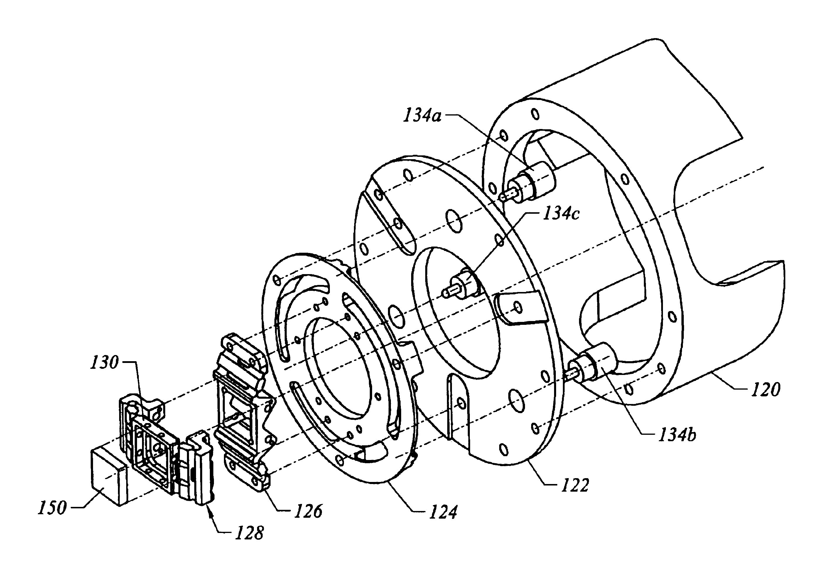
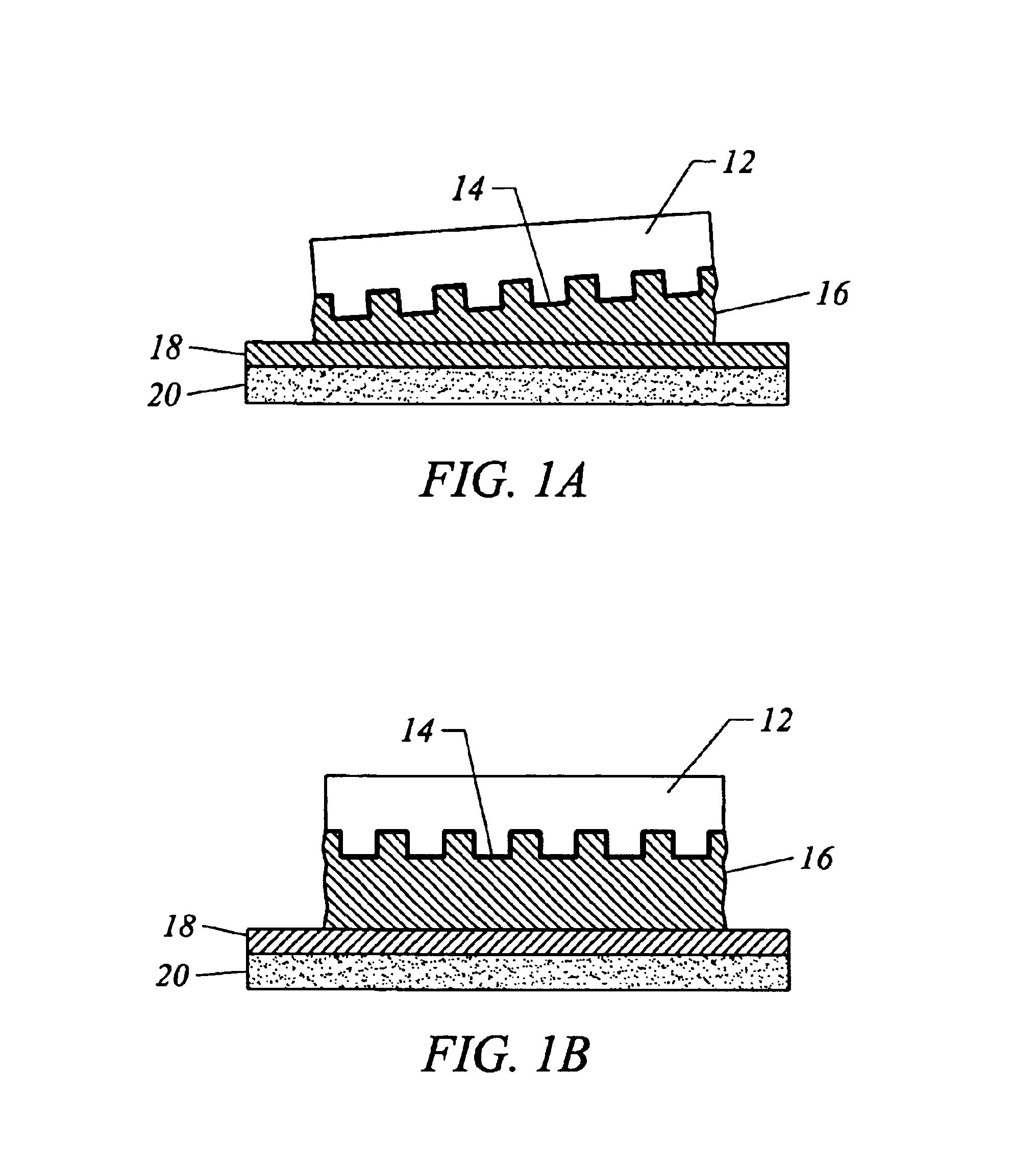
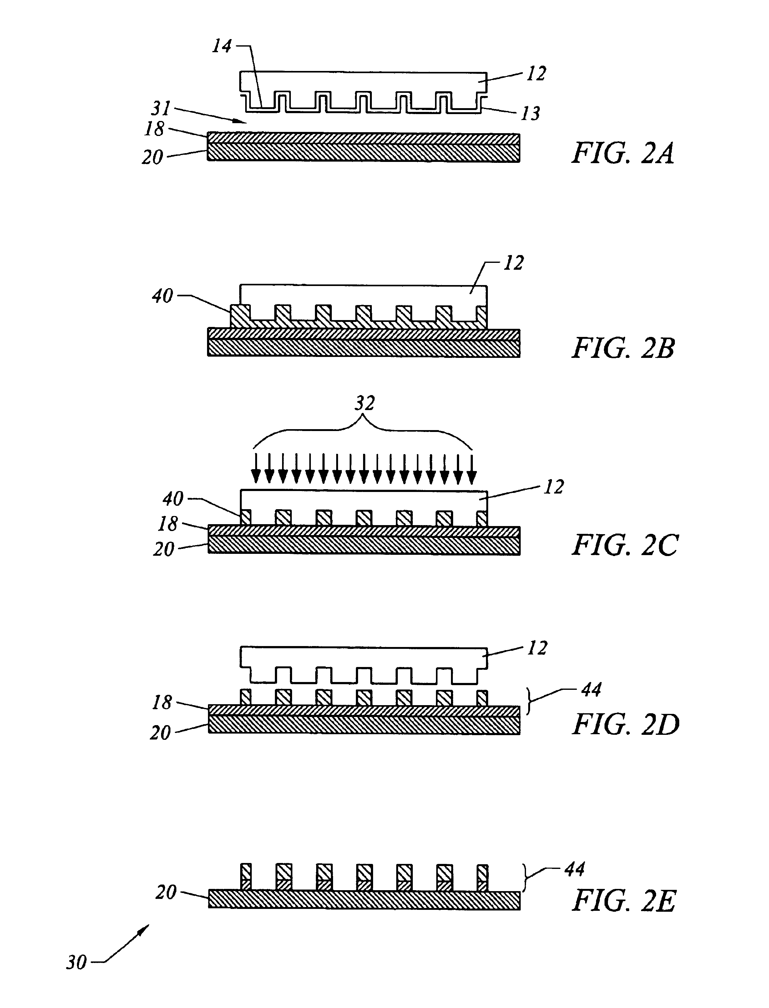
With reference now to the figures and specifically to FIGS. 1A and 1B, therein are shown arrangements of a template 12 predisposed with respect to a substrate 20 upon which desired features are to be imprinted using imprint lithography. Specifically, the template 12 includes a surface 14 that has been fabricated to take on the shape of desired features which, in turn, a...


PUM

PropertyMeasurementUnit
aspect ratioaaaaaaaaaa
forceaaaaaaaaaa
of rotationaaaaaaaaaa

Abstract

Processes and associated devices for high precision positioning of a template an substrate during imprint lithography includes a calibration system with a course calibration stage and a fine orientation stage capable of maintaining a uniform gap between the template and substrate. The fine orientation stage includes a pair of flexure members having flexure joints for motion about a pivot point intersected by first and second orientation axes. Actuators lengthen or shorten to expand or contract the flexure members. Separation of the template is achieved using a peel-and-pull method that avoids destruction of imprinted features from the substrate.

Description

TECHNICAL FIELDThe invention relates in general to techniques for small device manufacturing and specifically, to a system, processes and related devices for high precision imprint lithography enabling the manufacture of extremely small features on a substrate such as a semiconductor wafer. More specifically, the invention relates to methods and components for the orientation and alignment of a template about a substrate as well as their separation without destruction of imprinted features.BACKGROUND OF THE INVENTIONWithout limiting the invention, its background is described in connection with a process for the manufacture of sub-100 nm devices using imprint lithography.In manufacturing, lithography techniques that are used for large-scale production include photolithography and other application oriented lithography techniques such as electron beam lithography, ion-beam and x-ray lithography, as examples. Imprint lithography is a type of lithography that differs from these techniqu...

Claims


Application Information

Patent Timeline
Patent Type & Authority Patents(United States)
IPC IPC(8): G03F7/00G03F7/20G03F9/00H01L21/027H02N2/00
CPCB82Y10/00G03F9/00G03F7/0002B82Y40/00
Inventor CHOI, BYUNG JINSREENIVASAN, SIDLGATA V.JOHNSON, STEPHEN C.
Owner BOARD OF RGT THE UNIV OF TEXAS SYST
Why Eureka
Try Eureka