Electrostatic discharge protective circuitry equipped with a common discharge line

a protective circuitry and electrostatic discharge technology, applied in the direction of semiconductor devices, diodes, transistors, etc., can solve the problems of affecting the protection performance of the ic device, damage typically occurring during the testing phase of the device fabrication, and affecting the design of the device, so as to improve the protection performance. , the effect of improving the protection performan

Inactive Publication Date: 2005-03-29
UNITED MICROELECTRONICS CORP
View PDF2 Cites 16 Cited by
  • Summary
  • Abstract
  • Description
  • Claims
  • Application Information

AI Technical Summary

Benefits of technology

Another object of the present invention is to provide an ESD protection network having a triggering voltage and a holding voltage lower than that of the conventional design which can effectively make submicron IC devices immune

Problems solved by technology

An electrostatic charge may accumulate for various reasons and cause potentially destructive effects on an IC device.
Damage typically can occur during a testing phase of its fabrication, during assembly of the IC onto a circuit board, and during use of equipment into which the IC has been installed.
Damage to a single IC due to poor ESD protection in an electronic device can hamper some of its designed functions, or sometimes all of them.
ESD protection for semiconductor ICs is, therefore, a reliability problem.
Accordingly, such a prodigious network consumes a great amount of layout area, especially when used in a configuration including multi-power buses.
Moreover, no ESD protection is provided between any two IC pads using the conventional design.
However, the ESD pulse will boost the electric potential at the power rails, resulting in potential damage to the internal circuitry. K. Narita et al. have proposed another ESD protection circuit design in their article entitled “A NOVEL ON-CHIP E

Method used


Image

  • Electrostatic discharge protective circuitry equipped with a common discharge line
  • Electrostatic discharge protective circuitry equipped with a common discharge line
  • Electrostatic discharge protective circuitry equipped with a common discharge line

Examples


Embodiment Construction

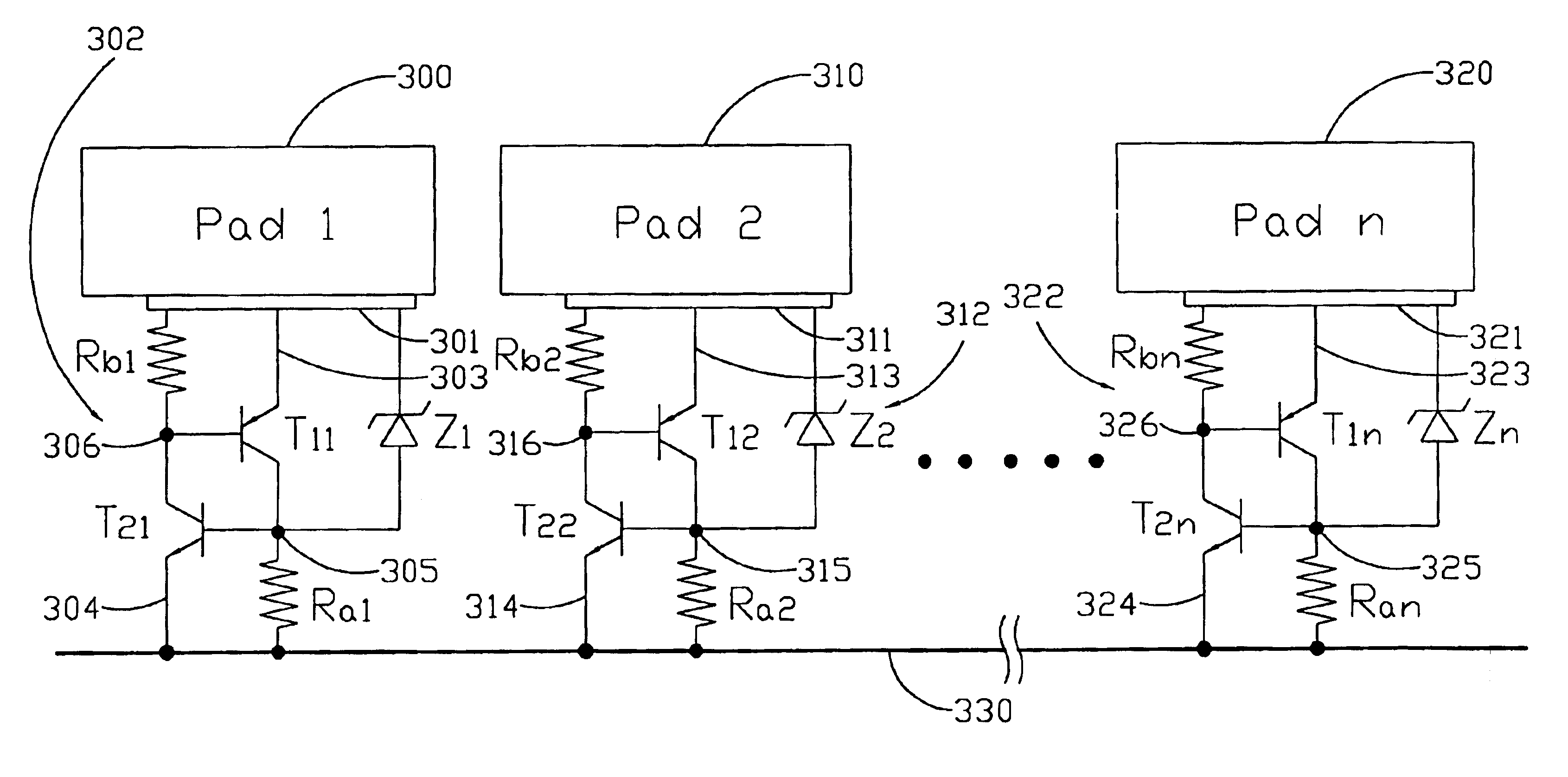
Before describing details of the present invention, a low triggering voltage SCR serves as the main component in an ESD protection circuit will be first described with reference to FIG. 2A and FIG. 2B. In both the drawings, the SCR device consists essentially of a PNP bipolar junction transistor T.sub.1 and an NPN bipolar junction transistor T.sub.2. The collector of the PNP transistor T.sub.1 is connected together with the base of the NPN transistor T.sub.2, forming a cathode gate identified by the node 200. The cathode gate 200 is coupled to the emitter of the NPN transistor T.sub.2, via a spreading resistor R.sub.a, constituting a cathode 201, which is connected to a ground terminal GND. The base of the PNP transistor T.sub.1 is connected together with the collector of NPN transistor T.sub.2 to form an anode gate identified by the node 202. The anode gate 202 is coupled to the emitter of the PNP transistor T.sub.1, via a spreading resistor R.sub.b, constituting an anode 203. To a...


PUM


Abstract

A semiconductor device having an electrostatic discharge protective circuitry adapted to a common discharge line (CDL) is disclosed. In the embodiments of the present invention, semiconductor device includes a plurality of bonding pads, each having at least one connecting terminal, a common discharge line, and a protective device connected between the connecting terminal and the common discharge line. Moreover, the protective device is composed of a silicon-control-rectifier that is used for electrostatic discharge protection and a zener diode for lowering a trigger voltage of the silicon-control-rectifier.

Description

FIELD OF THE INVENTIONThe present invention relates to a semiconductor device, and more particularly, to a semiconductor device having an electrostatic discharge protective circuitry adapted to a common discharge line (CDL).DESCRIPTION OF THE PRIOR ARTElectrostatic discharge (“ESD” hereafter) is a common phenomenon that occurs during handling of semiconductor IC devices. An electrostatic charge may accumulate for various reasons and cause potentially destructive effects on an IC device. Damage typically can occur during a testing phase of its fabrication, during assembly of the IC onto a circuit board, and during use of equipment into which the IC has been installed. Damage to a single IC due to poor ESD protection in an electronic device can hamper some of its designed functions, or sometimes all of them. ESD protection for semiconductor ICs is, therefore, a reliability problem. In order to prevent this, various electrostatic breakdown protection techniques have been proposed. As o...

Claims


Application Information

Patent Timeline
IPC IPC(8): H01L27/02
CPCH01L27/0262H01L27/0255
Inventor CHEN, SHIAO-SHIENTANG, TIEN-HAOWANG, MU-CHUN
Owner UNITED MICROELECTRONICS CORP
Why Eureka
Try Eureka