
Fault coverage and simplified test pattern generation for integrated circuits

Inactive Publication Date: 2005-03-29
QUALCOMM INC
View PDF4 Cites 4 Cited by
  • Summary
  • Abstract
  • Description
  • Claims
  • Application Information

AI Technical Summary

Benefits of technology

Accordingly, there is a need for a system and method for improved fault coverage and simplified test pattern generation for integrated circuits.

Problems solved by technology

Moreover, each could not exist in its present form without complex and powerful integrated circuits.
Because the wires and transistors within a modern integrated circuit are so small, a speck of dust that gets on the integrated circuit while it is being manufactured, or on the photographic masks or reticules used, is likely to make that particular integrated circuit chip fail to operate properly.
There are causes of manufacturing defects or faults other than dust and contaminants, but many of them affect only a single integrated circuit.
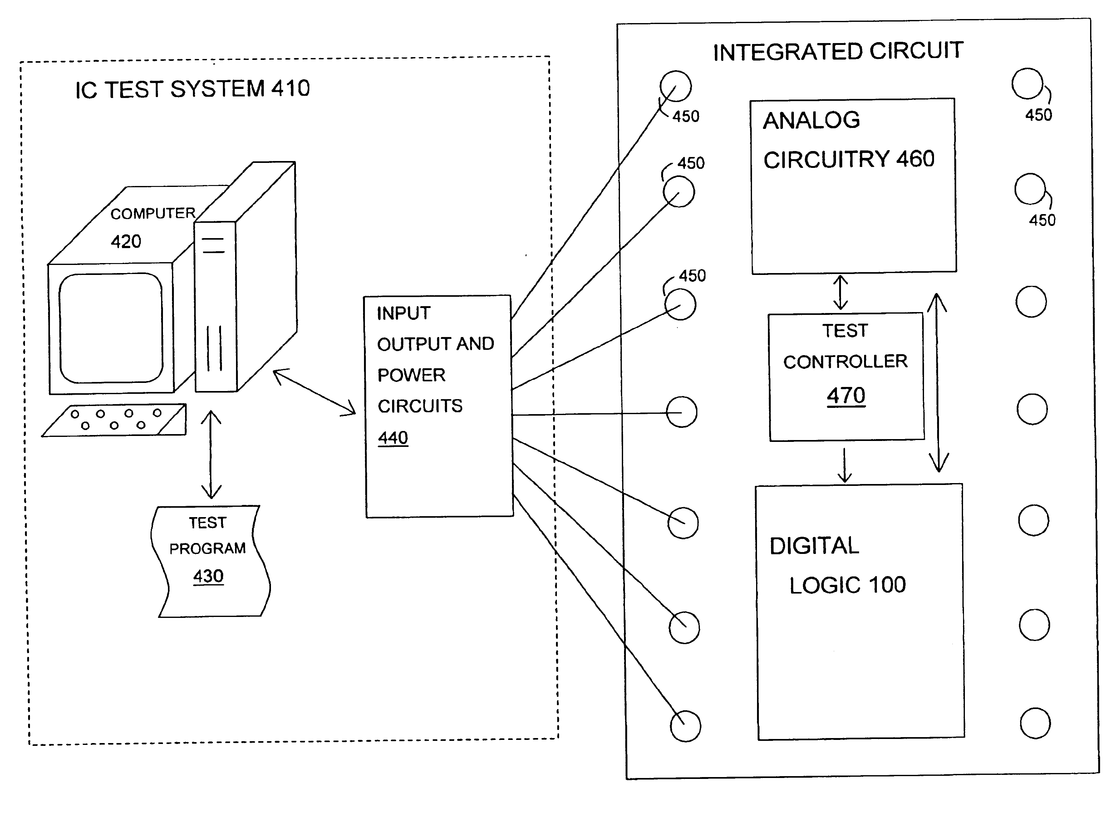
Because of this complexity, it can be difficult or impossible to develop a test program that thoroughly tests every combination of possible input signals, every device on the integrated circuit, or every feature that the integrated circuit implements in every mode in which the integrated circuit can be operated.
Even if such a program were available, it may be likely to be too lengthy to be practical; that is, it may not be economical to leave each integrated circuit in a sophisticated and expensive test system long enough to run the entire program.
However, test programs that cover faults at 95% of the nodes of a complex integrated circuit often have substantial drawbacks, including but not limited to:Running the test program on the integrated circuit tester often requires longer than desired to keep down the testing time, and thus keep down the cost of manufacturing the integrated circuit;Developing the test program often requires a substantial amount of engineering time; andThe test program often requires change or redesign every time that the, design of the integrated circuit is corrected or improved.

Method used


Image

  • Fault coverage and simplified test pattern generation for integrated circuits
  • Fault coverage and simplified test pattern generation for integrated circuits
  • Fault coverage and simplified test pattern generation for integrated circuits

Examples


Embodiment Construction

The descriptions, discussions and figures herein illustrate technologies related to the invention, show examples of the invention and give examples of using the invention. Known methods, procedures, systems, circuits or components may be discussed without giving details, so as to avoid obscuring the principles of the invention. On the other hand, numerous details of specific examples of the invention may be described, even though such details may not apply to other embodiments of the invention. Details are included and omitted so as to aid in understanding the invention.

The invention is not to be understood as being limited to or defined by what is discussed herein; rather, the invention may be practiced without the specific details described herein. One skilled in the art will realize that numerous modifications, variations, selections among alternatives, changes in form, and improvements can be made without departing from the principles, spirit or legal scope of the invention.

Some...


PUM


Abstract

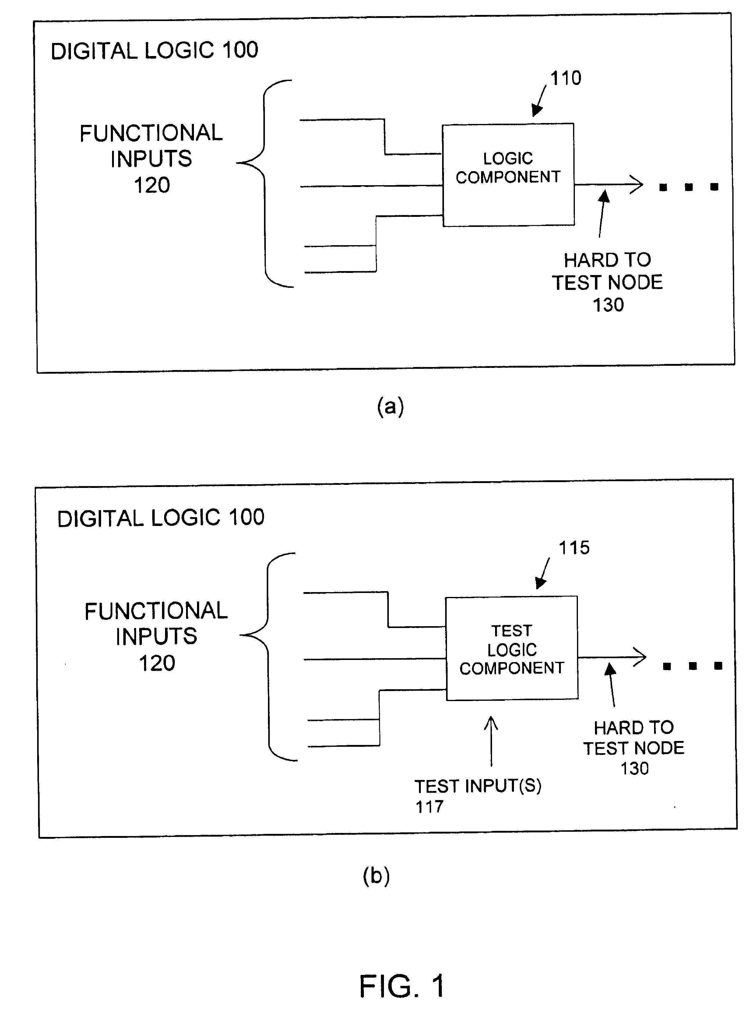
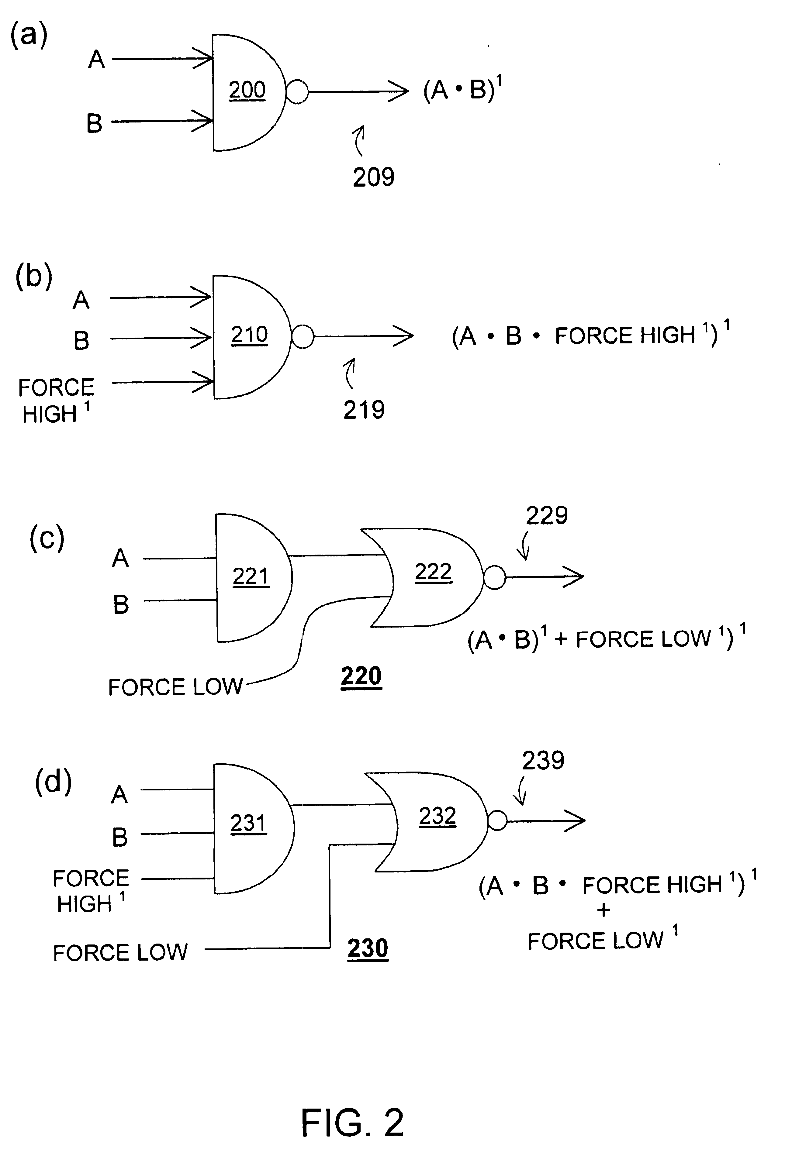
An integrated circuit with improved testability includes a test logic component that replaces a corresponding regular logic component and that generates a logic high or low whenever a test input is activated. Alternatively, it may generate either high or low depending on which of two test inputs is activated. A test program may be augmented with instructions to activate such test inputs. An integrated circuit design may be analyzed to select a node that is not covered by a test program and to identify which logic component generates an output on the node. Then the design may be altered to replace the identified logic component with a corresponding test logic component. Test coverage analysis may be based on determining whether the test program toggles the node, or determining whether a stuck at fault on the node propagates so as to be observed.

Description

BACKGROUND INFORMATION1. Field of the InventionThe present invention relates to the field of testing integrated circuits, and particularly to designing integrated circuits and their associated test programs so as to improve fault coverage.2. Description of Background ArtResearch and technology have provided society with a wide variety of electronic devices. Some modern electronic devices are powerful, and can be very beneficial to those who use them, or very enjoyable. Examples include, but are not limited to: personal computers (PCs), personal digital assistants (PDAs), pagers, mobile phones, portable music playback devices, or game systems. Each of these electronic devices contain one or more integrated circuits (ICs). Moreover, each could not exist in its present form without complex and powerful integrated circuits.An integrated circuit, or a chip as it is sometimes called, undergoes testing after it is manufactured and before it is assembled into an electronic device or system....

Claims


Application Information

Patent Timeline
IPC IPC(8): G01R31/28G01R31/3183
CPCG01R31/318307
Inventor SCHMITZ, LAWRENCE STANTON
Owner QUALCOMM INC
Learn More