Manufacturing method of a semiconductor device incorporating a passive element and a redistribution board

Inactive Publication Date: 2005-04-05
SOCIONEXT INC
View PDF13 Cites 39 Cited by
  • Summary
  • Abstract
  • Description
  • Claims
  • Application Information

AI Technical Summary

Benefits of technology

It is a general object of the present invention to provide an improved and useful manufacturing method o

Problems solved by technology

However, it is difficult to secure an area for mounting the bypass condenser on the package board close to the part where the semiconductor elements are mounted when mounting terminals for many signals and mounting terminals for power source and grounding are placed, or when a plurality of semiconductor elements are mounted on the package board as a system-in package.
However, a yield ratio may be reduced and an increase in costs may be caused since the number of wiring layers increases

Method used


Image

  • Manufacturing method of a semiconductor device incorporating a passive element and a redistribution board
  • Manufacturing method of a semiconductor device incorporating a passive element and a redistribution board
  • Manufacturing method of a semiconductor device incorporating a passive element and a redistribution board

Examples


first embodiment

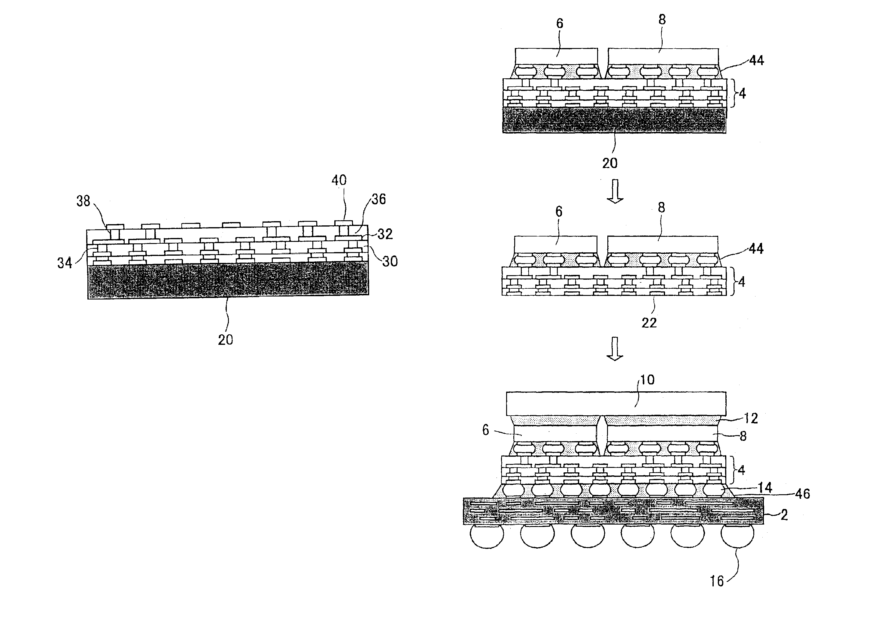
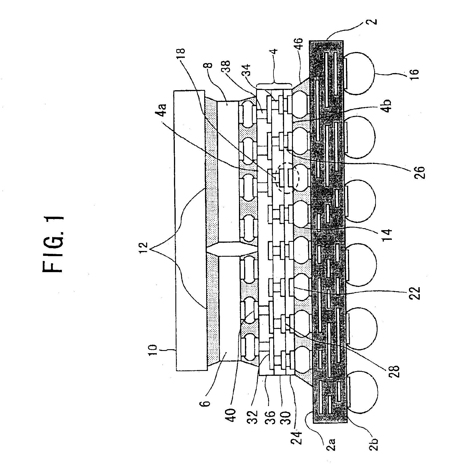
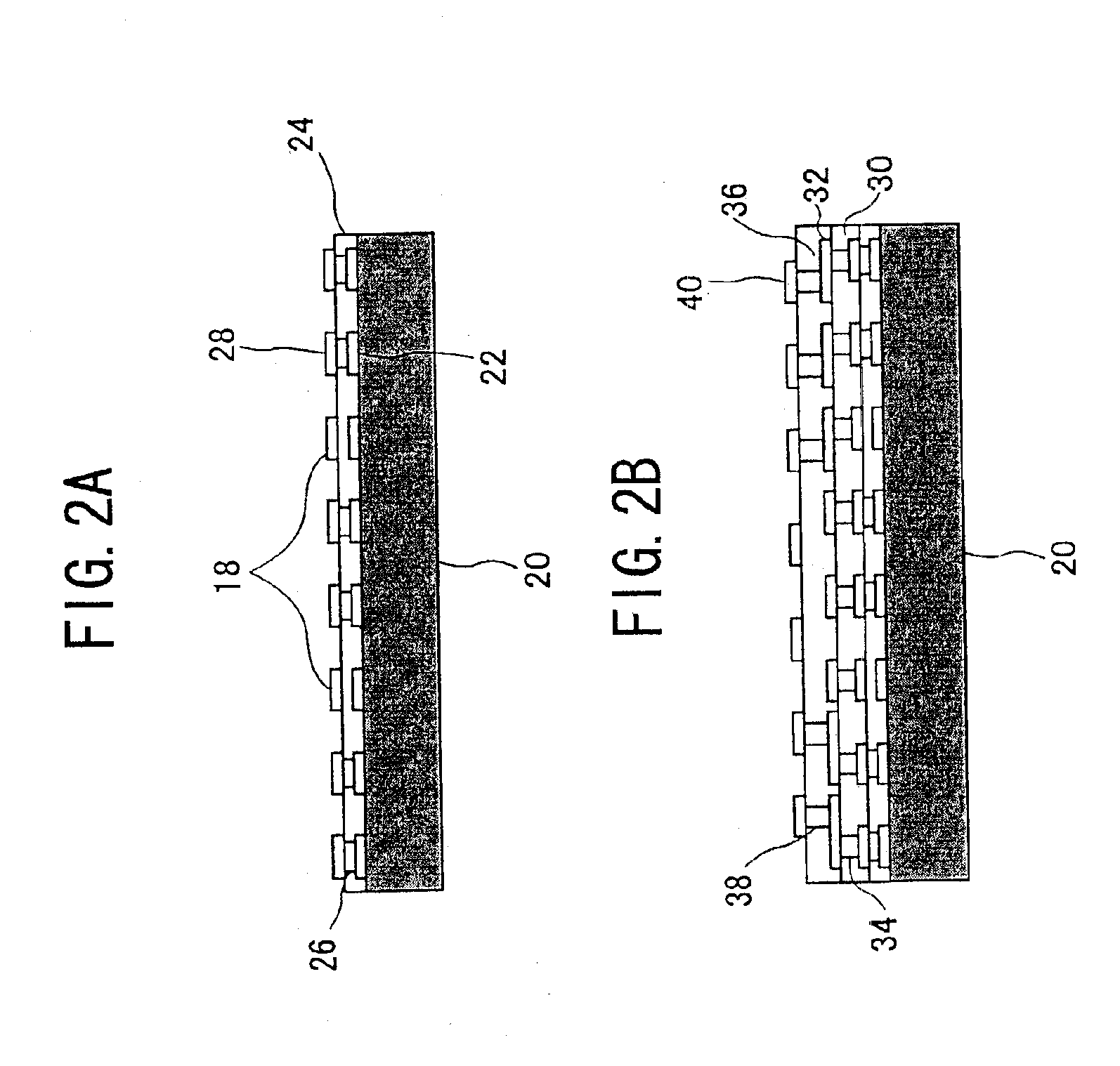
Next, in step S29, as shown in FIG. 6A, the redistribution board 4 is mounted on the package board 2. In step S30, the under fill material 46 is injected between the redistribution board 4 and the package board 2. Thereafter, in step S31, as shown in FIG. 6B, the base board 20 is removed. The base board 20 is removed by the same method as the above-described

As described above, in this embodiment, the redistribution board 4 is mounted on the package board 2 before the base board 20 is removed from the redistribution board 4. Thus, the redistribution board 4 is always reinforced by the base board 20 or the package board 2. Therefore, the deformation of or the damage to the redistribution board 4 due to the redistribution board 4 being by itself without any reinforcement can be prevented.

When the base board 20 is removed in step S31, the first electric conductive layer 22 is exposed from a surface of the redistribution board 4. Then, in step S32, the semiconductor elements 6 and 8 are ...

third embodiment

In the present invention, as shown in FIG. 8A, the redistribution board 4 is formed on the base board 20. Thereafter, as shown in FIG. 8B, the base board 20 is separated or removed from the redistribution board 4. Thereafter, the redistribution board 4 is bonded to the semiconductor elements 6 and 8 and the package board 2. As shown in FIG. 8C, the semiconductor elements 6 and 8 may be mounted on the redistribution board 4 previous to the package board 2. Or, as shown in FIG. 8D, the package board 2 may be mounted on the redistribution board 4 previous to the semiconductor elements 6 and 8. In this case, the redistribution board 4 is formed with a thickness to have enough strength even when the base board 20 is separated or removed. Alternatively, a material with enough strength is chosen to form the redistribution board 4.

Next, a description will be given of a fourth embodiment of the present invention with reference to FIG. 9. FIG. 9 is a cross sectional view of a semiconductor de...

fourth embodiment

The semiconductor device according to this embodiment has the same components as the semiconductor device according to the above-described fourth embodiment, except that the redistribution board 4A is placed upside down. That is, the metal pillars 50 of the redistribution board 4A are connected with the electrode pads of the package board 2. The semiconductor elements 6 and 8 are mounted on the electrode pads made of the electric conductive layer 22.


PUM


Abstract

A manufacturing method of a semiconductor device incorporating a passive element includes the steps as follows: a redistribution board forming step forms a redistribution board incorporating the passive element on a base board; a semiconductor element mounting step mounts at least one semiconductor element formed on an opposite side surface of the redistribution board with regard to the base board; a base board separating step separates the base board from the redistribution board and exposes the other surface of the redistribution board; a redistribution board mounting step mounts the redistribution board on a package board via electrode pads exposed from the other surface of the redistribution board.

Description

BACKGROUND OF THE INVENTION1. Field of the InventionThe present invention generally relates to a semiconductor device mounting a logic device and the like that requires high-speed processing, and more particularly, to a semiconductor device incorporating a passive element such as a capacitor in a package.2. Description of the Related ArtGenerally, in a semiconductor device mounting an LSI that operates at high speed, a bypass condenser is incorporated in a package board in order to prevent variation of power supply voltage and malfunction due to high-frequency noise, and to secure stable operation in a high-speed operation area.The bypass condenser is mounted on the package board as a different chip part from a semiconductor element that is mounted on the package board by flip chip mounting (FC mounting). In order to make the bypass condenser function effectively, it is necessary to place the bypass condenser near the semiconductor element. In many cases, the bypass condenser is pla...

Claims


Application Information

Patent Timeline
IPC IPC(8): H01L25/065H01L23/498H01L23/36H01L23/48H01L23/34H05K1/14H01L21/56H01L21/02H05K1/16H01L23/12H01L21/68
CPCH01L23/36H01L23/49811H01L23/49816H01L23/49822H01L23/49833H01L25/0655H05K1/141H01L21/6835H01L21/563H01L2224/16235H01L2221/68345H01L2224/1134H01L2224/13099H01L2224/16225H01L2224/73253H01L2924/01046H01L2924/01078H01L2924/01079H01L2924/09701H01L2924/15311H01L2924/15312H01L2924/19041H05K1/162H05K2201/049H05K2201/10734H05K2201/10977H01L2224/32225H01L2924/01019H01L2924/00013H01L2224/73204H01L2924/00014H01L2924/00H01L2224/45144H01L2224/05573H01L2224/05568
Inventor YONEDA, YOSHIYUKIMINAMIZAWA, MASAHARUSHIMIZU, NOBUTAKAIMAMURA, KAZUYUKIKIKUCHI, ATSUSHINUKIWA, MASARUYAMAGUCHI, OSAMUFUJIMOTO, YASUNORIIHARA, TAKUMIMORIOKA, MUNEHARUKURIKI, YUKIHIROUCHIDA, MASAKI
Owner SOCIONEXT INC
Why Eureka
Try Eureka