Semiconductor device and process for manufacturing the same

a semiconductor and semiconductor technology, applied in the field of semiconductor devices, can solve the problems of complex manufacturing process, significant increase in gate overlap capacitance, and inhibit the improvement of the operating speed of mis transistors

Inactive Publication Date: 2005-04-05
PANASONIC CORP
View PDF12 Cites 29 Cited by
  • Summary
  • Abstract
  • Description
  • Claims
  • Application Information

AI Technical Summary

Problems solved by technology

According to the above MIS transistor, thinning the gate insulating film 101 allows for low-voltage operation and increases the current drive capability, however, it causes the following problems because the gate electrode 102 is composed of polysilicon.
This problem is also attributed to the fact that there is a solid solubility limit for the impurity contained in the gate electrode 102, which is composed of polysilicon.
Such a significant i

Method used


Image

  • Semiconductor device and process for manufacturing the same
  • Semiconductor device and process for manufacturing the same
  • Semiconductor device and process for manufacturing the same

Examples


first embodiment

(First Embodiment)

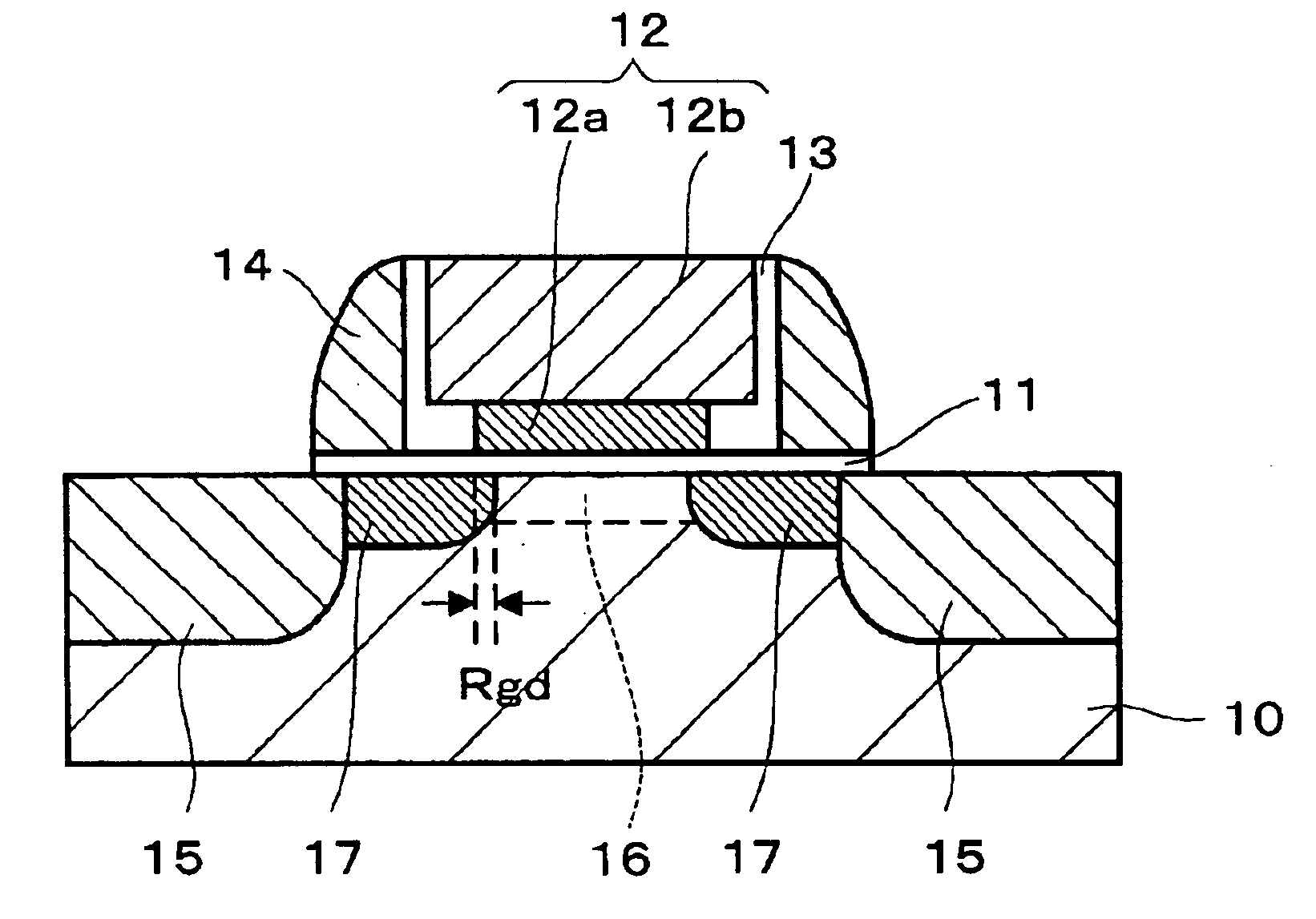
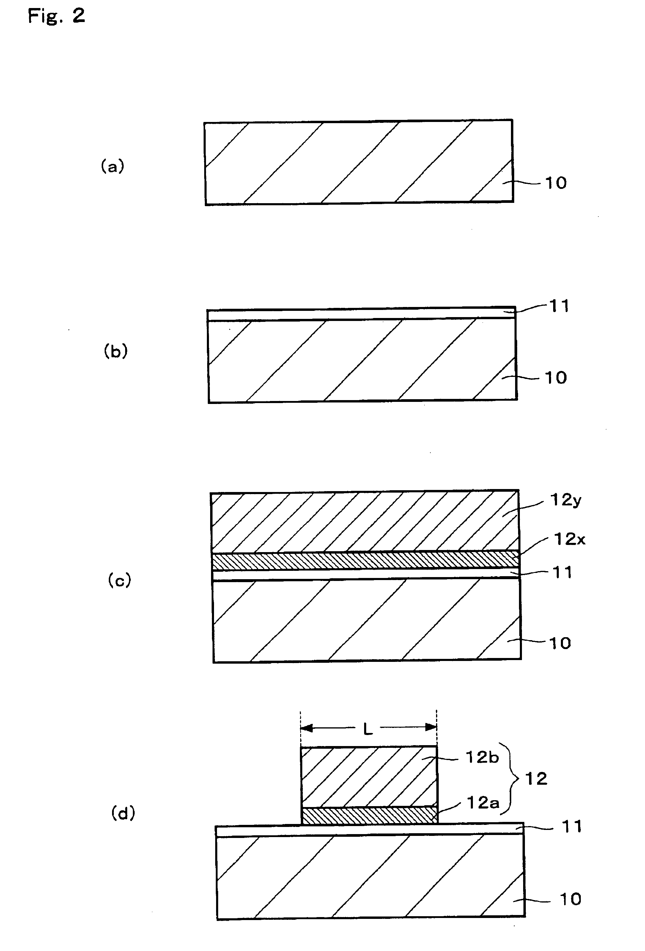
The first embodiment of the present invention will be described below. FIG. 1 is a cross-sectional view of a semiconductor device of the present embodiment.

As illustrated in the figure, this semiconductor device is an MIS transistor, and comprises an Si substrate 10 and a gate electrode 12 formed on the substrate 10 via a gate insulating film 11. The gate insulating film 11 is composed of silicon oxide, and has a thickness of about 2 nm. The gate electrode 12 is composed of a lower gate electrode element 12a formed on the gate insulating film 11 and an upper gate electrode element 12b formed thereon. The lower gate electrode element 12a includes a p-type impurity (e.g., boron) in high concentration, and is composed of polycrystalline SiGe (with a Ge composition ratio of about 50%) with a thickness of about 50 nm. The upper gate electrode element 12b includes a p-type impurity (e.g., boron) in high concentration, and is composed of polycrystalline Si with a thicknes...

second embodiment

(Second Embodiment)

The second embodiment of the present invention will now be described. FIG. 5 is a cross-sectional view of a semiconductor device according to the present embodiment.

The semiconductor device of the present embodiment is identical to that of the first embodiment in terms of the structure of the gate electrode, but is different in terms of the structure of the substrate on which the gate electrode is formed. The equivalent structural elements are therefore provided with the same reference numerals. Also, the detailed explanations for the equivalent elements are omitted.

As illustrated in FIG. 5, in the semiconductor device of the present embodiment, the substrate on which the gate electrode is formed has a structure in which an SiGe film 21 with a thickness of about 15 nm is formed by epitaxial growth on an Si substrate 10, and an Si film 22 with a thickness of about 5 nm is formed thereon by epitaxial growth. A gate electrode 12 is formed on the Si film 22 via a gate...

third embodiment

(Third Embodiment)

The third embodiment of the present invention will now be described. FIG. 10 is a cross-sectional view of a semiconductor device according to the third embodiment of the present invention.

As illustrated in FIG. 10, the semiconductor device of the present embodiment is a CMIS device with a dual-gate structure, and comprises a shallow trench isolation (STI) region, and an n-well 30 and a p-well 50 formed in the two regions separated from each other by the STI region. A p-channel MIS transistor (pMISFET) is provided above the n-well 30, while an n-channel MIS transistor (nMISFET) is provided above the p-well 50.

The pMISFET comprises a gate insulating film 31 formed on the n-well 30 and a gate electrode 32 formed thereon. The gate insulating film 31 is composed of silicon oxide and has a thickness of about 2 nm. The gate electrode 32 is composed of a lower gate electrode element 32a formed on the gate insulating film 31 and an upper gate electrode element 32b formed th...


PUM


Abstract

This specification relates to a process for manufacturing a semiconductor device, comprising the steps of: forming a lower gate electrode film on a semiconductor substrate 10 via a gate insulating film 11; forming an upper gate electrode film on the lower gate electrode film, the upper gate electrode film being made of a material having a lower oxidation rate than that of the lower gate electrode film; forming a gate electrode 12 by patterning the upper gate electrode film and the lower gate electrode film, the gate electrode 12 comprising a lower gate electrode element 12a and an upper gate electrode element 12b; forming source/drain regions 15 by introducing an impurity into the semiconductor substrate 10; and forming oxide film sidewalls 13 by oxidizing the side faces of the lower gate electrode element 12a and the upper gate electrode element 12b, the thickness of the oxide film sidewalls 13 in the gate length direction being larger at the sides of the lower gate electrode element 12a than at the sides of the upper gate electrode element 12b.

Description

TECHNICAL FIELDThe present invention relates to a semiconductor device having an MIS transistor structure, and a process for manufacturing the same.BACKGROUND ARTIn recent years, the scaling of CMOS devices, such as the reduction of the gate length in MIS transistors or the thinning of gate insulating films, has allowed for improvements in operating speed and integration. In particular, MIS transistors having a gate insulating film with a thickness of 2 nm or less or a gate electrode with a gate length of about 50 nm have recently been developed.FIG. 11 is a cross-sectional view of a conventional MIS transistor. As shown in the figure, this MIS transistor comprises an Si substrate 100 and a gate electrode 102 formed thereon via a gate insulating film 101 composed of silicon oxide. The gate electrode 102 is composed of polysilicon, and has oxide film sidewalls 103 formed on its side faces. The Si substrate 100 includes high-impurity-concentration source / drain regions 104 formed at th...

Claims


Application Information

Patent Timeline
IPC IPC(8): H01L21/70H01L21/28H01L21/02H01L29/10H01L29/66H01L21/321H01L29/78H01L29/02H01L21/8238H01L29/40H01L29/49H01L29/80
CPCH01L21/2807H01L21/28105H01L21/28114H01L21/28247H01L21/32105H01L21/823807H01L29/802H01L21/82385H01L21/823864H01L29/1054H01L29/4983H01L29/7836H01L21/823842
Inventor TAKAGI, TAKESHI
Owner PANASONIC CORP
Why Eureka
Try Eureka