High-frequency switch, and electronic device using the same

a high-frequency switch and electronic device technology, applied in the direction of coupling devices, electric devices, transistors, etc., can solve the problems of difficult use, high signal frequency, and limit the shape of the inductance device, so as to achieve low insertion loss and high signal cut-off properties

Inactive Publication Date: 2005-04-05
MURATA MFG CO LTD
View PDF10 Cites 130 Cited by
  • Summary
  • Abstract
  • Description
  • Claims
  • Application Information

AI Technical Summary

Benefits of technology

The present invention has been made to solve the above-described problems, and accordingly, provides a high-frequency switch and an electronic device using the same which can be used up to high frequencies, with little insertion loss when switching on, and with high signal cut-off properties when switching off.
With the high-frequency switch according to the present invention, the switch acts to cut off the high-frequency signals flowing through the main line electrode by grounding a portion of the main line electrode by turning this FET on, and conducting the high-frequency signals flowing through the main line electrode by turning this FET off. The main line electrode exists only at a part of the FET, so insertion loss when switching on can be reduced. Also, a grounding state with no frequency properties can be realized, so the high-frequency signals can be cut off in a stable manner when switching off. Consequently, high isolation properties can be obtained.
Further, with the electronic device according to the present invention, reduction in power consumption and in malfunctions can be realized by using the high-frequency switch according to the present invention.

Problems solved by technology

However, there is a limit to how far the shape of the inductance device can be reduced with the same level of precision in inductance value.
Further, the higher the signal frequency is, the smaller the inductance value needs to be, so there is the problem with this configuration that the higher the signal frequency is, the harder it is to use.
On the other hand, with the second conventional example, the above problem, wherein the higher the signal frequency is the harder the device is to use, does not occur since the resonance phenomenon is not used.
Accordingly, with switches wherein the main line itself is the drain electrode for the FET as with the first conventional example, this arrangement is a factor in increasing insertion loss of the main line.
Also, the on resistance per increment length of the FET can be reduced by changing the cross-sectional structure of the FET, which is not necessarily easy.
Increasing the gate width of the FET means extending the gate electrode in the longitudinal direction of the signal line, which in turn means that the drain electrode also becomes longer, resulting in an increased size of the switch in the longitudinal direction of the main line.
Next, the third conventional example has been same basic configuration as with the first conventional example, and has the same problems.
However, there is the need to lengthen the gate width of the FET to obtain grounding with sufficiently low resistance for the stub end.
Having different resonance frequencies for an open stub and short stub means that the switch cannot function normally, which is a great problem.

Method used


Image

  • High-frequency switch, and electronic device using the same
  • High-frequency switch, and electronic device using the same
  • High-frequency switch, and electronic device using the same

Examples


Embodiment Construction

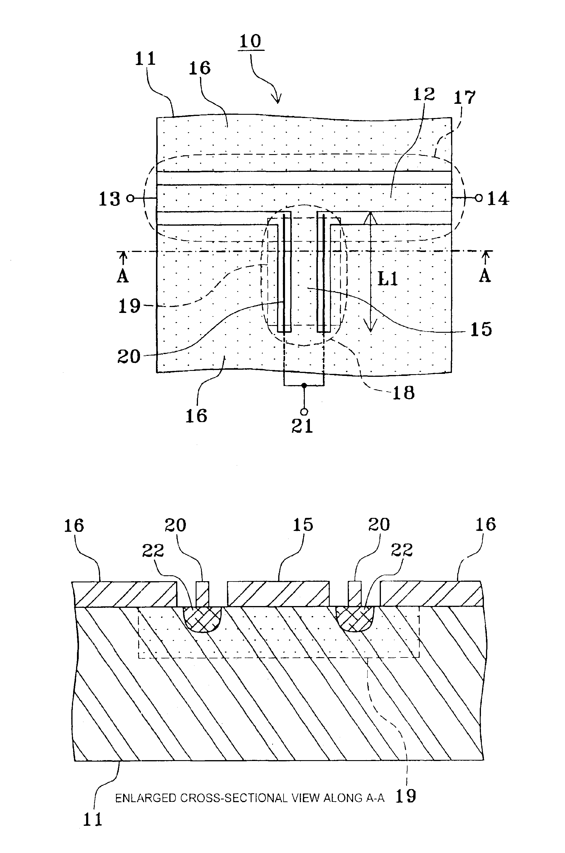
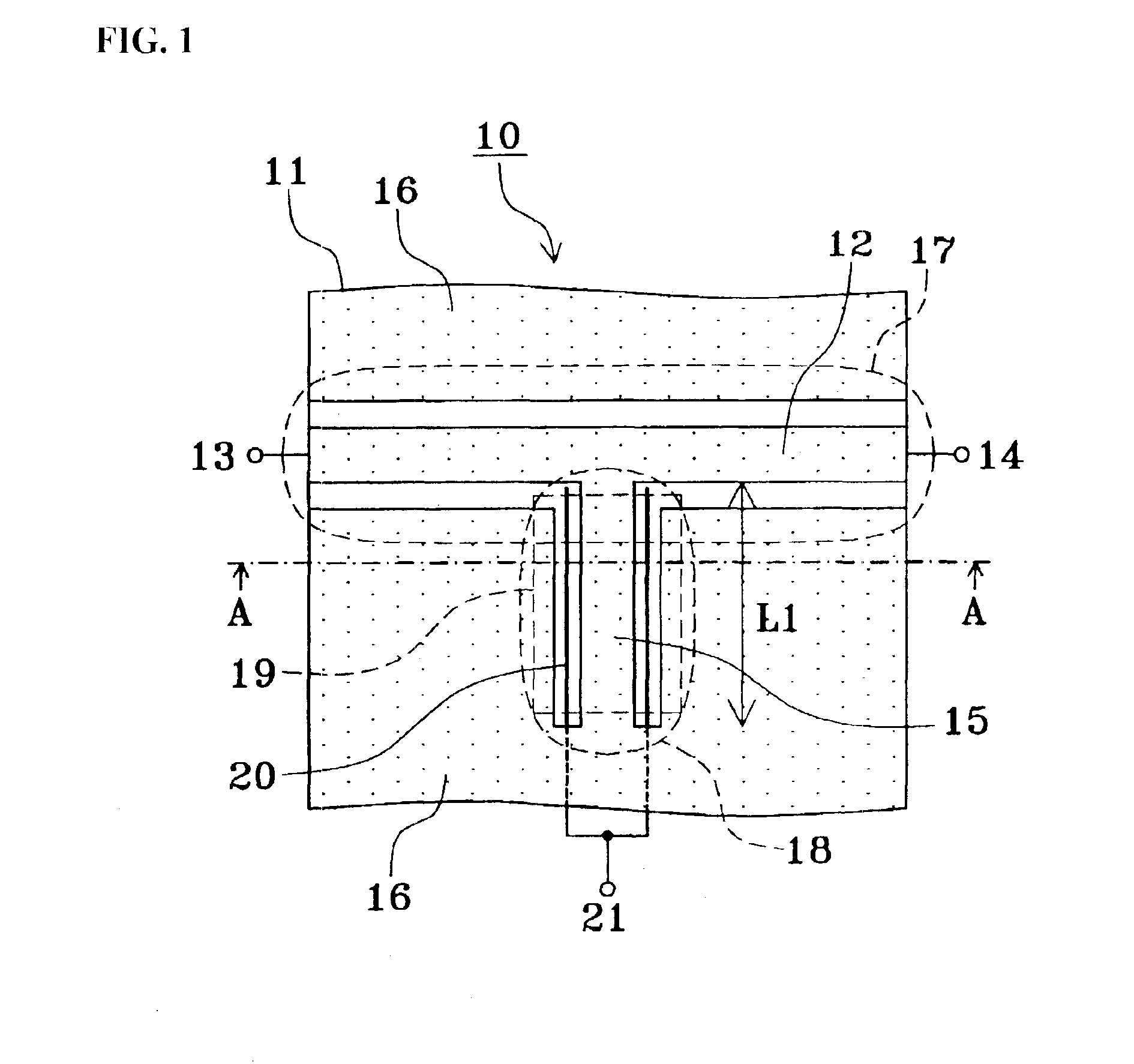
FIG. 1 is a plan view illustrating an embodiment of a high-frequency switch according to the present invention, and FIG. 2 is an enlarged view of a cross-section along line A—A of the high-frequency switch shown in FIG. 1.

In FIG. 1, a high-frequency switch 10 has a main line 17 and stub 18 formed of a coplanar wave guide formed on a semiconductor substrate 11. The main line 17 is formed of a main line electrode 12 and ground electrodes 16 formed on both sides thereof in the width direction, with one end and the other end being connected to terminals 13 and 14, respectively. The stub 18 is formed of a stub line electrode 15 and ground electrodes 16 formed on both sides thereof in the width direction, with one end connected to the main line 17, and the other end connected to the ground electrode 16 so as to be grounded. Or, in more precise terms, one end of the stub line electrode 15 of the stub 18 is connected to the side edge of the main line electrode 12 of the main line 17, and th...


PUM


Abstract

A high-frequency switch comprises: a substrate; a main line electrode provided between two terminals; a stub line electrode with one end thereof connected to the side edge of the main line electrode and the other end thereof grounded; and a ground electrode provided adjacent to the stub line electrode in the width direction thereof; wherein the substrate has a semiconductor activation layer which extends to below the stub line electrode and the ground electrode between at least one side edge of the stub line electrode and the ground electrode; and wherein a gate electrode which extends in the longitudinal direction of the stub line electrode is provided on the semiconductor activation layer between the stub line electrode and the ground electrode, thereby forming an FET structure, thus providing a high-frequency switch and electronic device therewith, capable of using high frequencies, having reduced insertion loss, and high signal cut-off capabilities.

Description

BACKGROUND OF THE INVENTION1. Field of the InventionThe present invention relates to a high-frequency switch and an electronic device using the same, and particularly to a high-frequency switch used for switching millimeter bandwidth signals and an electronic device using the same.2. Description of the Related ArtGenerally, switches using PIN diodes are used for switching millimeter bandwidth signals and so forth. Switches using FETs may be used for relatively low frequencies, such as switches which use the lines themselves where high-frequency signals pass, as the drain and source of the FETs. Specific examples are disclosed in Japanese Unexamined Patent Application Publication No. 6-232601, Japanese Unexamined Patent Application Publication No. 10-41404, Japanese Unexamined Patent Application Publication No. 2000-294568, Japanese Unexamined Patent Application Publication No. 2000-332502, and so forth.Japanese Unexamined Patent Application Publication No. 6-232601 (first convention...

Claims


Application Information

Patent Timeline
Patent Type & Authority Patents(United States)
IPC IPC(8): H01P1/10H01P1/15H01L27/095
CPCH01P1/15
Inventor NAKANO, HIROYUKI
Owner MURATA MFG CO LTD
Why Eureka
Try Eureka