Nonvolatile memory, verify method therefor, and semiconductor device using the nonvolatile memory

a non-volatile memory and verify method technology, applied in static storage, digital storage, instruments, etc., can solve the problems of reducing the speed of verify operation, affecting the speed of verification operation, and essentially taking a long time to verify operation

Inactive Publication Date: 2005-04-05
SEMICON ENERGY LAB CO LTD
View PDF4 Cites 5 Cited by
  • Summary
  • Abstract
  • Description
  • Claims
  • Application Information

AI Technical Summary

Benefits of technology

[0014]A fundamental idea underlying the present invention is that, to realize a high-speed verify operation, there is avoided the repetition of writing/erasing and reading, which has been a factor of consuming

Problems solved by technology

However, the conventional verify operation necessitates the repetition of writing/erasing and reading, which leads to a problem that this verify operation essentially takes long time in comparison with a single operation in which reading is not performed.
Further, an operation voltage in the writing/erasing becomes high in comparison with a case of reading,

Method used


Image

  • Nonvolatile memory, verify method therefor, and semiconductor device using the nonvolatile memory
  • Nonvolatile memory, verify method therefor, and semiconductor device using the nonvolatile memory
  • Nonvolatile memory, verify method therefor, and semiconductor device using the nonvolatile memory

Examples


embodiments

[0127]Embodiments of the present invention will be described below.

first embodiment

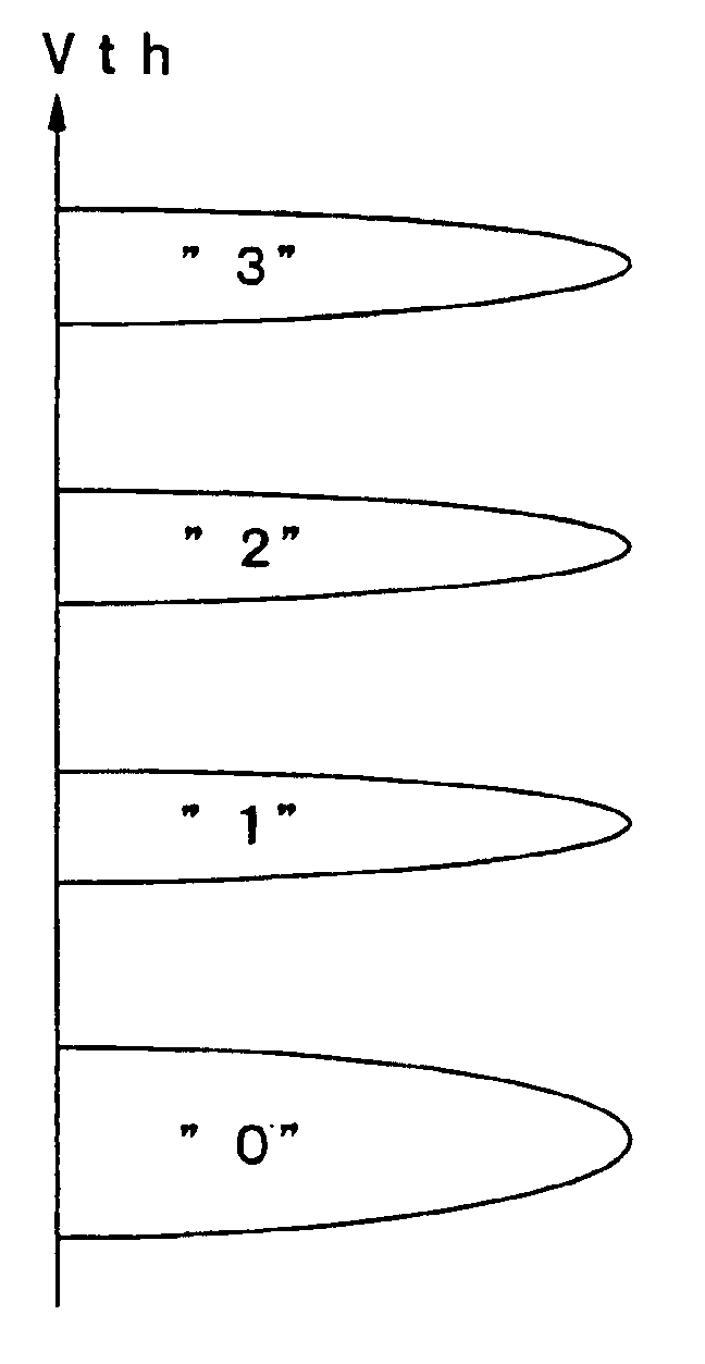
[0128]There will be described an embodiment in which the constant verify scheme of the present invention is applied to a binary NOR-type nonvolatile memory constructed of n-channel type memory elements. In this embodiment, there will be described a case where there are adopted the one-line simultaneous writing and bit-by-bit verify scheme by the HE injection and the one-line simultaneous erasing and bit-by-bit verify scheme by the FN discharge.

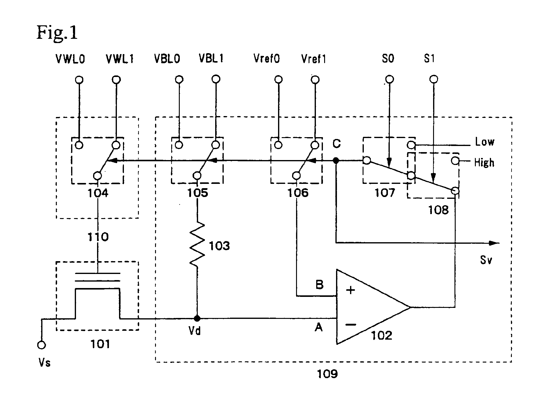
[0129]As an example of the block circuit diagram of the nonvolatile memory of this embodiment, it is possible to use the block circuit diagram in FIG. 10 that has been described in the above embodiment mode. Accordingly, there will be omitted the description of the circuit constructions of the memory cell array 1001, the X selector 1002, and the X address decoder 1003. The bit line driving circuit 1004 that has the operation circuits (1) to (n) and the operation circuit 1005 will be described after the description of operation voltages.

[0130]F...

second embodiment

[0154]There will be described an embodiment in which the constant verify scheme of the present invention is applied to a binary NOR-type nonvolatile memory constructed of p-channel type memory elements. In this embodiment, there will be described a case of adopting the one-line simultaneous writing and bit-by-bit verify scheme by the FN injection and the one-line simultaneous erasing and bit-by-bit verify scheme by the FN discharge.

[0155]An example of the block circuit diagram of the nonvolatile memory in this embodiment is shown in FIG. 15. The memory cell array shown in FIG. 15 has a circuit construction, in which memory elements connected in parallel to form one row is divided into a plurality of blocks, and is also called the “AND-type nonvolatile memory”.

[0156]The block circuit diagram shown in FIG. 15 is constructed of a memory cell array 1501 in which memory cells are arranged in an m-line by n-row matrix manner (m and n are each integers equal to or more than one), a word li...


PUM


Abstract

Provided is a nonvolatile memory that realizes a high-speed verify operation. During verify writing/erasing, the writing/erasing and reading are performed at the same time. As to a circuit that performs a verify operation, for instance, there is obtained a construction where the output from a sense amplifier (102) that performs reading is connected to a switch which switches an operation voltage applied to a memory cell in accordance with a verify signal Sv, and the verify operation is finished concurrently with having the verify signal Sv switched. By obtaining such circuit construction and simultaneously performing writing/erasing and reading, it becomes possible to perform high-speed verify writing/erasing.

Description

[0002]This application is a continuation of U.S. application Ser. No. 10 / 131,840, filed on Apr. 25, 2002 now U.S. Pat. No. 6,768,680.BACKGROUND OF THE INVENTION[0003]1. Field of the Invention[0004]The present invention relates to a semiconductor nonvolatile memory. In particular, the present invention relates to an electrically writable and erasable semiconductor nonvolatile memory (also referred to as the “EEPROM” or “electrically erasable and programmable read only memory”). Also, the present invention relates to a semiconductor device which has the semiconductor nonvolatile memory.[0005]It should be noted here that the term “electrically writable and erasable semiconductor nonvolatile memory (EEPROM)” refers to a whole of semiconductor nonvolatile memories that are electrically writable and electrically erasable, and examples thereof include an EEPROM that is capable of performing erasing on a bit-by-bit basis and a flash memory. Also, unless being specified, the terms “nonvolati...

Claims


Application Information

Patent Timeline
IPC IPC(8): G11C16/34G11C16/06G11C16/04G11C16/02
CPCG11C16/3468G11C16/3481G11C16/3472
Inventor KATO, KIYOSHI
Owner SEMICON ENERGY LAB CO LTD
Why Eureka
Try Eureka