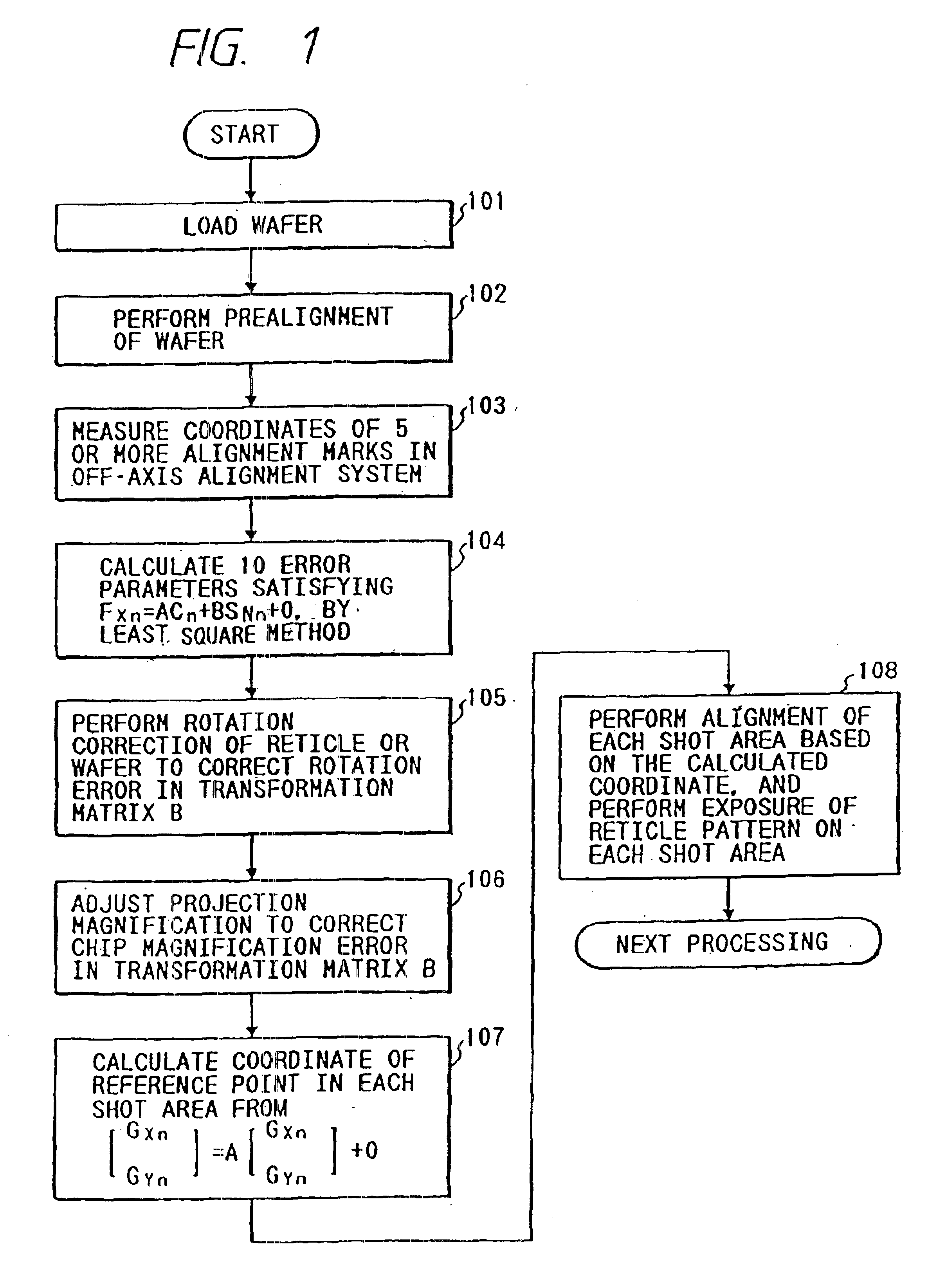
However, when superposing another pattern on the pattern formed previously, even though the
wafer is subjected to the stepping operation based on the predetermined arrangement coordinate values, sufficient alignment accuracy cannot be necessarily obtained owing to the following factors.
However, even though the
wafer is positioned in accordance with the calculated alignment coordinate value upon calculation (FXn, FYn), sufficient alignment accuracy cannot be necessarily obtained owing to the following factors.
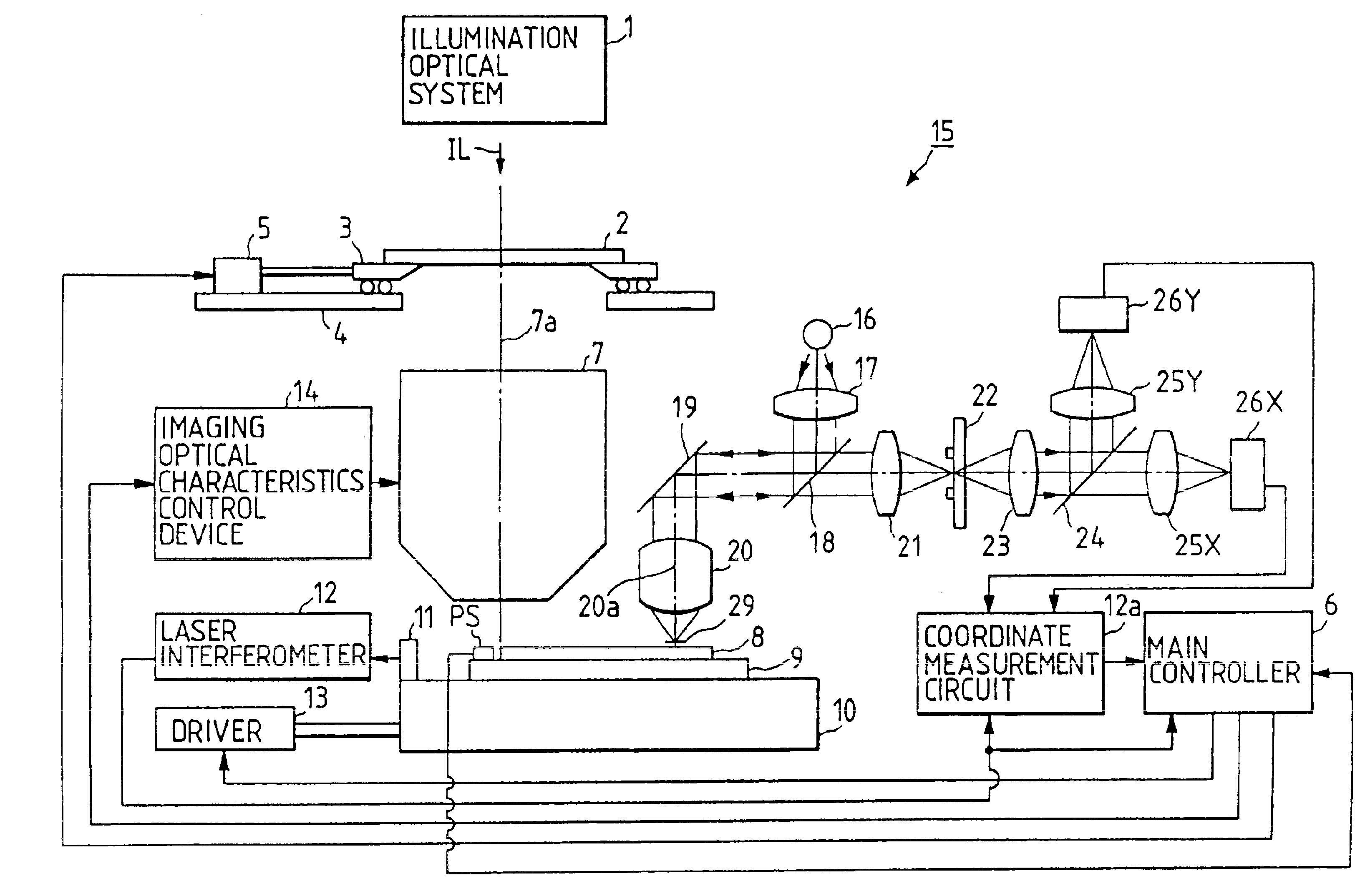
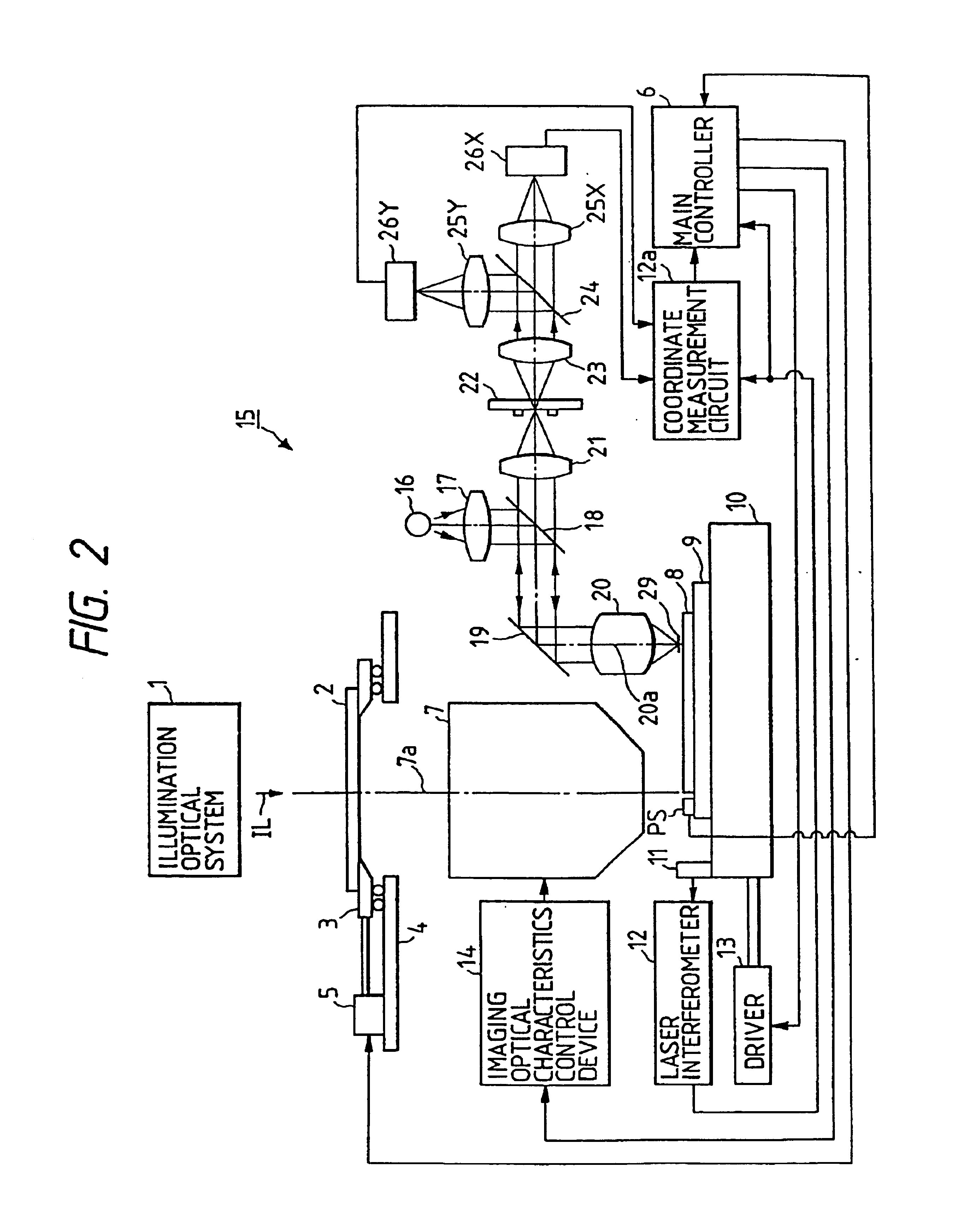
These are caused by the deviation or rotation of the reticle from a predetermined position, the projection
magnification error of the projection optical
system or the
distortion of the projection optical
system when the
chip pattern is first (first layer) printed on each shot area on the wafer.
Furthermore, these factors are changed by the
distortion occuring at the time of processing the wafer.
Further, there is presented such a
disadvantage that when a reticle is rotated or translated, a pattern image of the reticle and a
chip pattern on a wafer cannot be precisely aligned with each other.
However, the former method offers such a problem that it is difficult to drive the rotational error into a value below a predetermined allowable value due to an error in depiction of the marks on the reticle.
Further, the latter method offers such a problem that
exposure operation for forming the latent images greatly lowers the through-put.
Further, another
disadvantage occurs such that the pattern image of the reticle cannot precisely be aligned with the
chip pattern on the wafer over their entire surfaces due to an error in the projection
magnification of the
projection system.
However, there is present a problem in which this method has to use the reticle exclusively for measurement so that a relatively long time is required for the measurement of the
magnification, causing the through-put to be greatly lowered, and further, it is difficult to precisely measure the projection magnification due to an error in the depiction of the reticle.
However, according to the off-axis method, a measured position and an
exposure position are separated comparatively widely, which results in a poor through-put (the number of wafers processed per unit time).
However, when an alignment sensor of the LIA method or the LSA method is used, errors may be generated in measurement results of a scaling (a linear expansion or contraction of the entire wafer) and a magnification of a chip pattern within a shot area, under the influence of the asymmetric configuration generated on the surface of the wafer mark formed, for example, by aluminum vapor deposition on the wafer.
There is a possibility that extent of these influences differ from one another for each lot due to non-uniformity of the process so that it is inconveniently difficult to compensate these influences only with the constants obtained in advance.

