

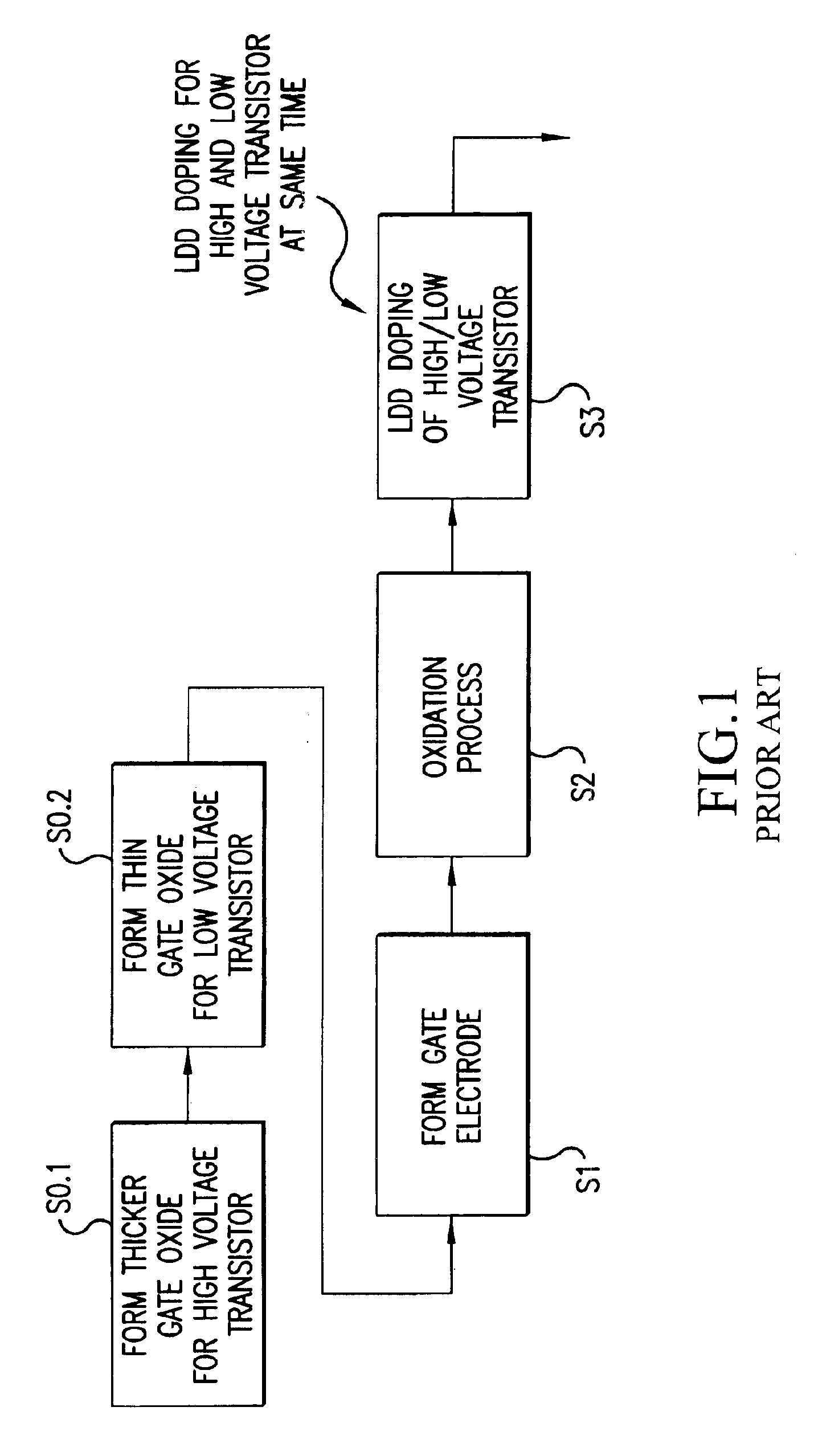
Low volt/high volt transistor
a low-voltage, transistor technology, applied in the direction of transistors, semiconductor devices, electrical equipment, etc., can solve the problems of reducing low-voltage transistors, and low-voltage transistors, so as to enhance the reliability of high-voltage transistors and short-channel effect immunity
- Summary
- Abstract
- Description
- Claims
- Application Information
AI Technical Summary
Benefits of technology
Problems solved by technology
Method used
Image

Examples
Embodiment Construction
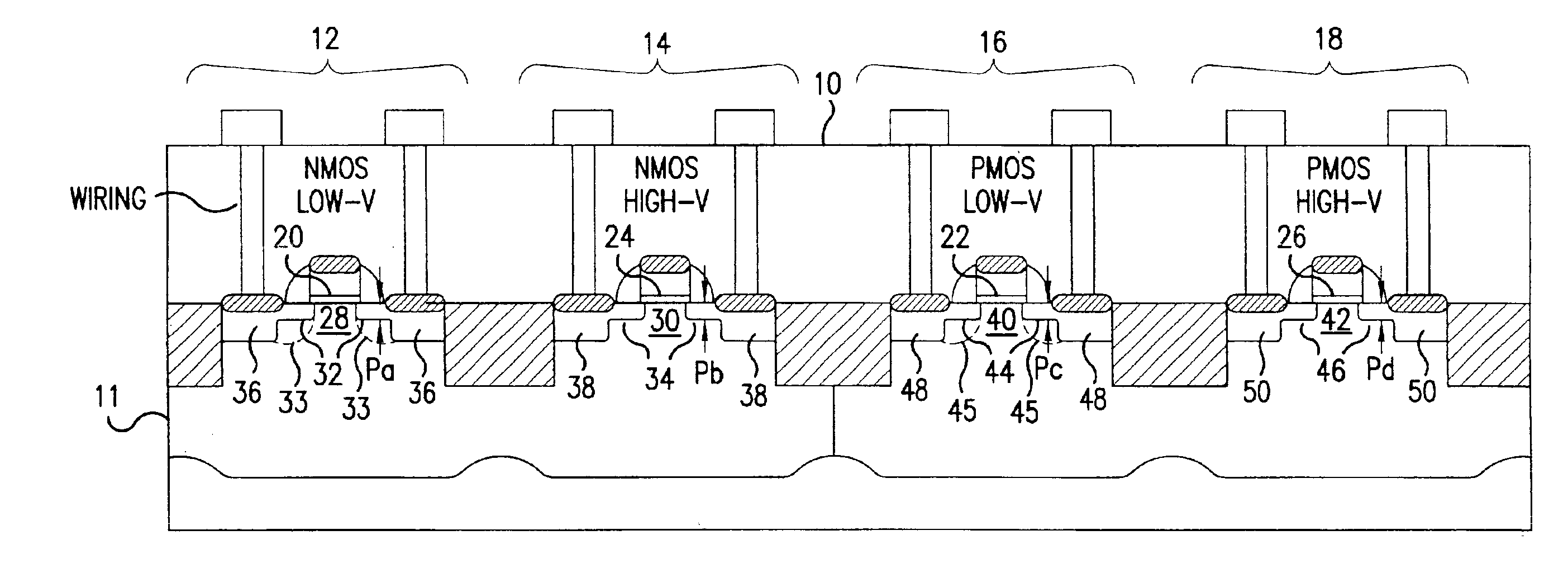
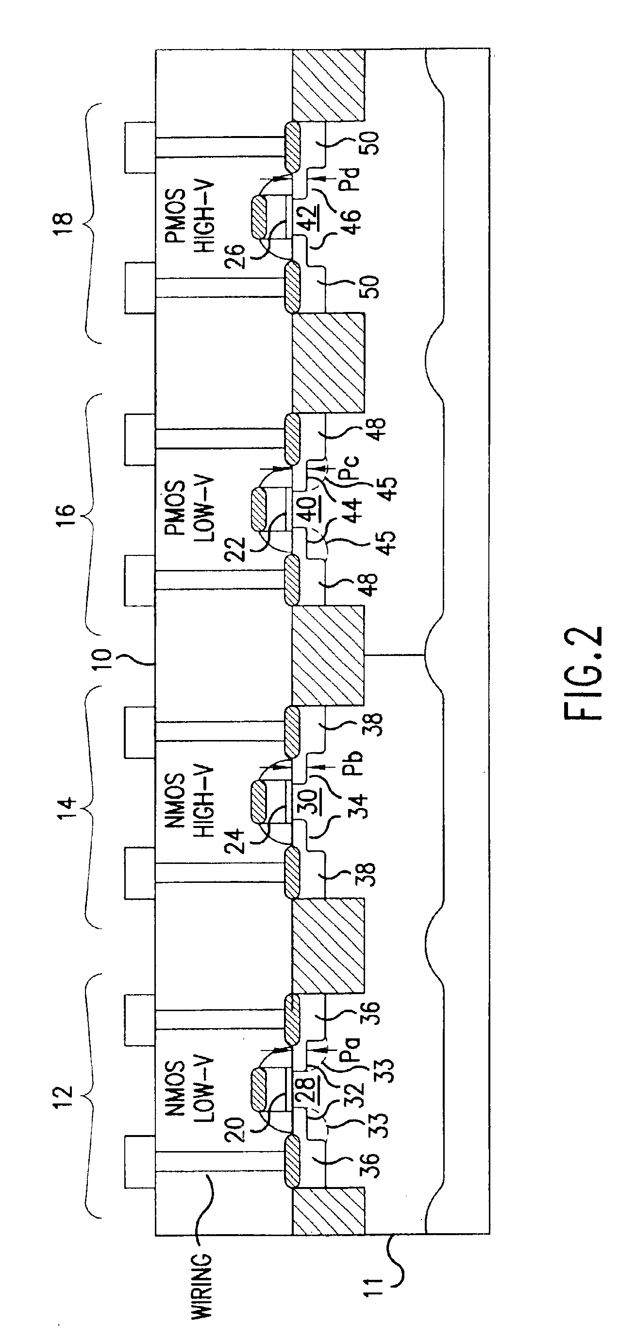
[0021]The invention provides a semiconductor device having low-voltage / high-voltage transistors and a method for forming low-voltage / high-voltage transistors of semiconductor devices for use in large scale integrated circuits (LSI), for example. In the method, and preferably on an LSI where at least one low-voltage transistor is intermingled with a high-voltage transistor, a low-density doping (LDD) implantation of the high-voltage transistor is conducted. Then, a protective oxide film for the LDD implantation of the low-voltage transistor is formed using a suitable oxidation process such as thermal oxidation or thermal chemical vapor deposition (CVD). Thereafter, LDD implantation of the low-voltage transistor is conducted.
[0022]With the method of the invention, a deep junction is obtained in the LDD region of the high-voltage transistor because, after LDD implantation, the oxidation process (thermal oxidation / thermal CVD) is applied, causing any impurities to diffuse. Moreover, any...
PUM
 Abstract
Description
Claims
Application Information