
Multi-stage collector having electrode stages isolated by a distributed bypass capacitor

a bypass capacitor and collector technology, applied in the direction of klystrons, amplifiers with transit-time effect, transit-tube circuit elements, etc., can solve the problem of rf leakage from the inside of the collector, and achieve the effect of improving energy efficiency

Inactive Publication Date: 2005-04-12
E2V TECH (UK) LTD
View PDF6 Cites 3 Cited by
  • Summary
  • Abstract
  • Description
  • Claims
  • Application Information

AI Technical Summary

Benefits of technology

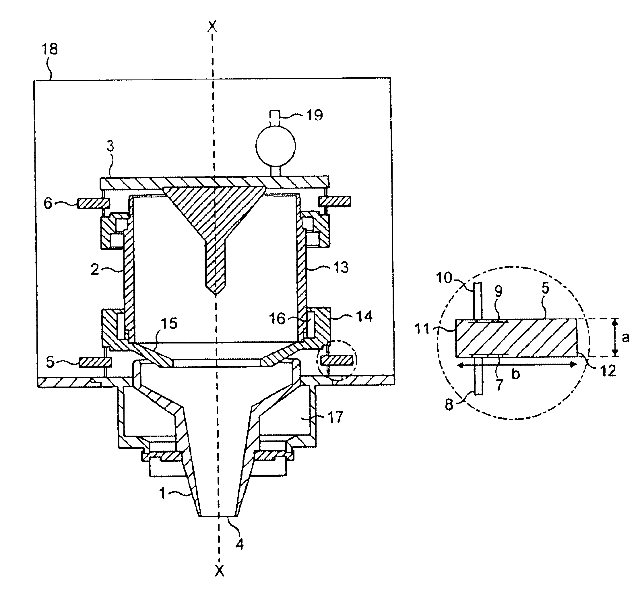
The ring is an annulus, the radial distance between its outer and inner peripheries being equal to or greater than the axial distance between its end faces. This is in contrast to a conventional arrangement in which electrical insulation between adjacent electrode stages is provided by a dielectric cylinder having a significant axial length compared to the thickness of its wall. By using the invention, the ring enables a high capacitance to be achieved as the distance between the plates is small compared to their surface area. Thus the combination of the ring and the metal plates is able to perform as a bypass capacitor which is effective as a low impedance at high frequencies. The electron beam entering the collector is modulated by rf current components, generating rf voltages in the collector region. This can result in rf leakage occurring from the inside of the collector to the outside of the collector through insulators separating collector stages. Use of the invention permits rf leakage through the insulators to be reduced or eliminated compared to a conventional construction. Preferably the ring is of a ceramic material, but other forms of insulator may be suitable.
Advantageously, at least one of the metal plates does not extend to the inner and outer peripheries of the face on which it is located. Thus, in addition to the axial thickness of the ring providing a certain path length between components at different electrical potentials, there is also the distance between the edge of the metal plate and the periphery. It is therefore possible to obtain the same voltage hold-off with the dielectric ring as would be possible with a dielectric cylinder of greater axial length. This also provides a more compact collector in the axial direction.
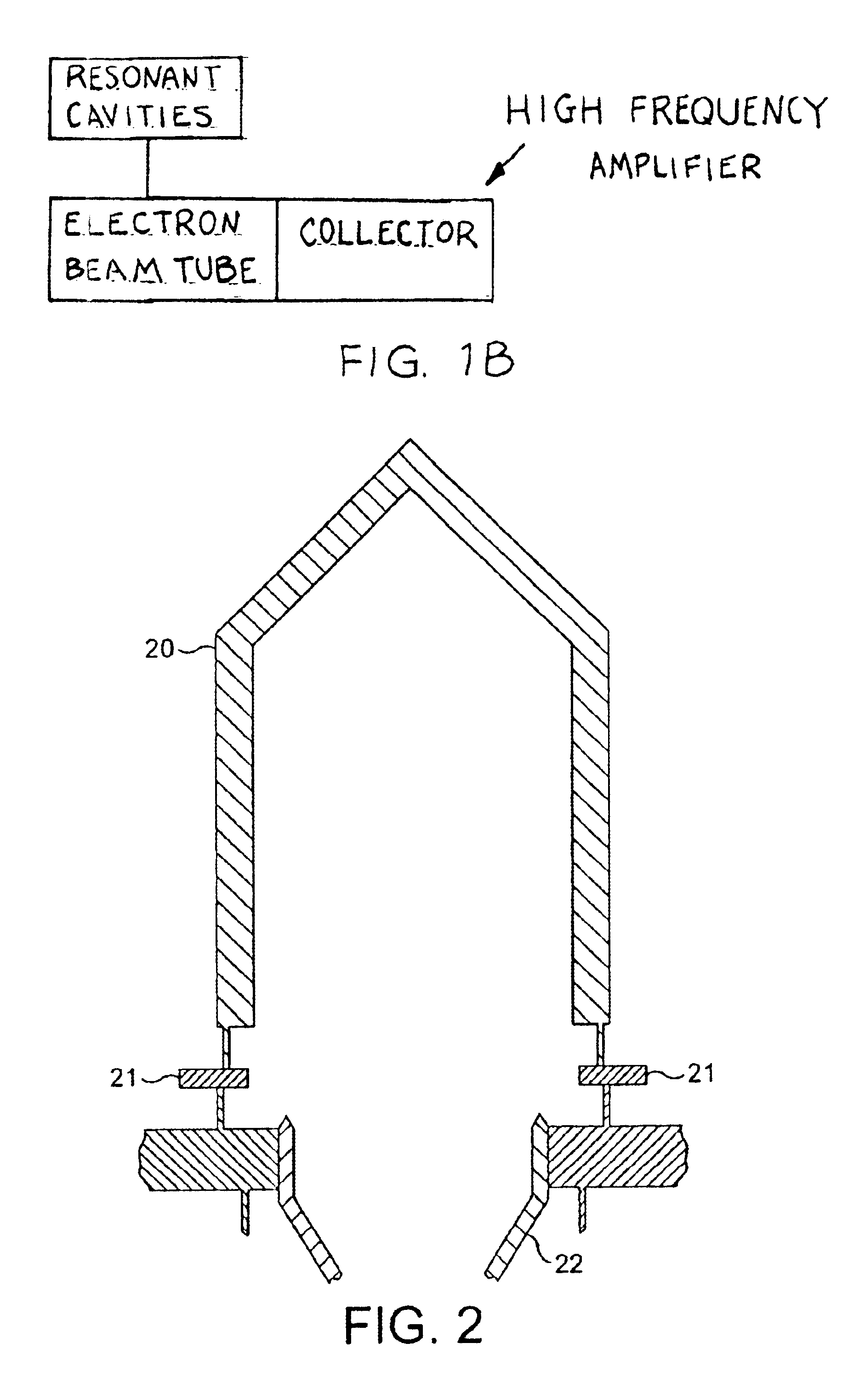
The invention maybe applied to a collector formed as a single piece, with the dielectric ring being located between the collector and the body of the tube to which it is fixed. The distributed bypass capacitor is thus defined by the collector body, ring and tube body. Thus, a further aspect of the invention provides an electron beam tube comprising two stages, one of which is a collector, with a dielectric ring between them, the ring having a respective metal plate on each of its end faces electrically connected to the respective stages such that, together with the ring, they define a high-frequency bypass capacitor. This arrangement may be advantageous where the collector is operated at depressed voltage to give improved energy efficiency.

Problems solved by technology

This can result in rf leakage occurring from the inside of the collector to the outside of the collector through insulators separating collector stages.

Method used


Image

  • Multi-stage collector having electrode stages isolated by a distributed bypass capacitor
  • Multi-stage collector having electrode stages isolated by a distributed bypass capacitor
  • Multi-stage collector having electrode stages isolated by a distributed bypass capacitor

Examples


Embodiment Construction

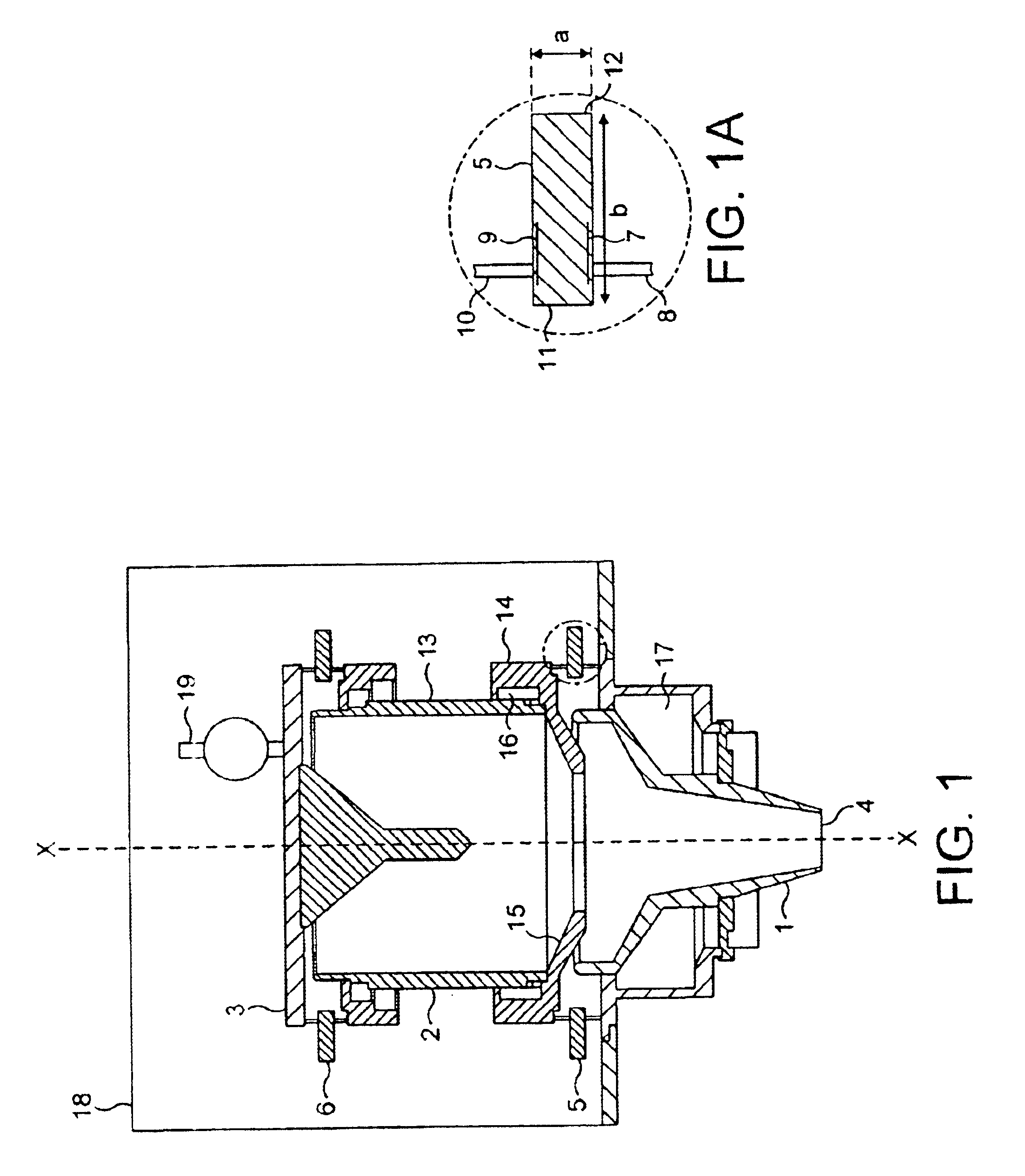
With reference to FIG. 1, a multi-stage electron beam collector includes a first electrode stage 1, second electrode stage 2 and a third electrode stage 3 arranged along a longitudinal axis X—X along which, during use, an electron beam enters the collector at opening 4 of the first stage 1, which also acts as the output drift tube.

A ceramic annular ring 5 is located between the first stage 1 and second stage 2 and another annular ceramic ring 6 between stages 2 and 3. As can be seen in FIG. 1A, the ring 5 includes a region of metallisation 7 on an end face. The metallisation is in electrical contact with a thin cylindrical metal wall 8 which is as at the same potential as the first stage 1 and thus effectively forms part of the first collector stage. Similarly, on the opposing end face of the ring 5 another layer of metallisation 9 is in electrical contact with a thin cylindrical wall 10 which forms part of the second stage 2. The ring 6 between the second and third stages 2 and 3 a...


PUM


Abstract

In a multistage collector used in a linear beam tube such as an IOT or klystron, electrode stages are separated by ceramic rings having metallised surfaces to provide distributed bypass capacitors. This eliminates or reduces leakage or any radio frequency energy from the interior of the collector to the outside.

Description

BACKGROUND OF THE INVENTIONThis invention relates to collectors for electron beam tubes.Linear electron beam tubes are used for the amplification of rf signals. They incorporate an electron gun for the generation of an electron beam of the appropriate power. The electron gun has a cathode heated to a high temperature so that the application of an electric field results in the emission of electrons, the electric field being produced by spacing an anode in front of and some distance from the cathode. Typically, the anode is held at around potential and the cathode at a large, for example, several tens of kilovolts, negative potential.In one type of linear beam tube called an Inductive Output Tube (IOT), a grid is placed close to and in front of the cathode and an rf signal to be amplified is applied between the cathode and grid so that the electron beam generated in the gun region is density modulated. The density modulated electron beam is directed through an rf interaction region wh...

Claims


Application Information

Patent Timeline
Patent Type & Authority Patents(United States)
IPC IPC(8): H01J23/02H01J23/027H01J23/54H01J23/00
CPCH01J23/0275H01J23/54H01J2225/10H01J2225/04
Inventor WILSON, ROBERTBARDELL, STEVENCROMPTON, TIMOTHY A
Owner E2V TECH (UK) LTD
Learn More