Semiconductor memory device with sense amplifier

Inactive Publication Date: 2005-04-12
RENESAS ELECTRONICS CORP
View PDF4 Cites 11 Cited by
  • Summary
  • Abstract
  • Description
  • Claims
  • Application Information

AI Technical Summary

Benefits of technology

An object of the present invention is to provide a semiconductor memory device that can be reduced in chip area (an area necessary for forming an element) while preventing degradation of characteristic.
In this manner, the subdecoder region is used as a region in which a sense amplifier driver element is arranged, so that the area of the sense amplifier region can be reduced as compared with a case where a sense amplifier driver element is arranged with the sense amplifier-forming element in the sense amplifier region. Furthermore, the sense amplifier driver element is arranged in a region (the subdecoder region) other than the sense amplifier region, the degree of freedom of arrangement of the sense amplifier-forming element in the sense amplifier region can be increased.

Problems solved by technology

Therefore it has become difficult to arrange all the elements constituting a sense amplifier driving circuit at an intersection region.
As a result of efficiently arranging the components in the region in which the sense amplifier is arranged as described above, however, the shapes of N-well and P-well that are required to arrange the element such as P-channel MOS transistor and N-channel transistor have often been complicated.
This may lead to degradation in characteristic of the semiconductor memory device.

Method used


Image

  • Semiconductor memory device with sense amplifier
  • Semiconductor memory device with sense amplifier
  • Semiconductor memory device with sense amplifier

Examples


Embodiment Construction

In the following, an embodiment of the present invention will now be described with reference to the figures. It is noted that in the figures the same or corresponding parts will be denoted with the same reference numerals and description thereof will not be repeated.

Referring to FIGS. 1-5, a semiconductor memory device in accordance with the embodiment of the present invention will be described.

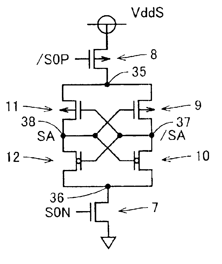
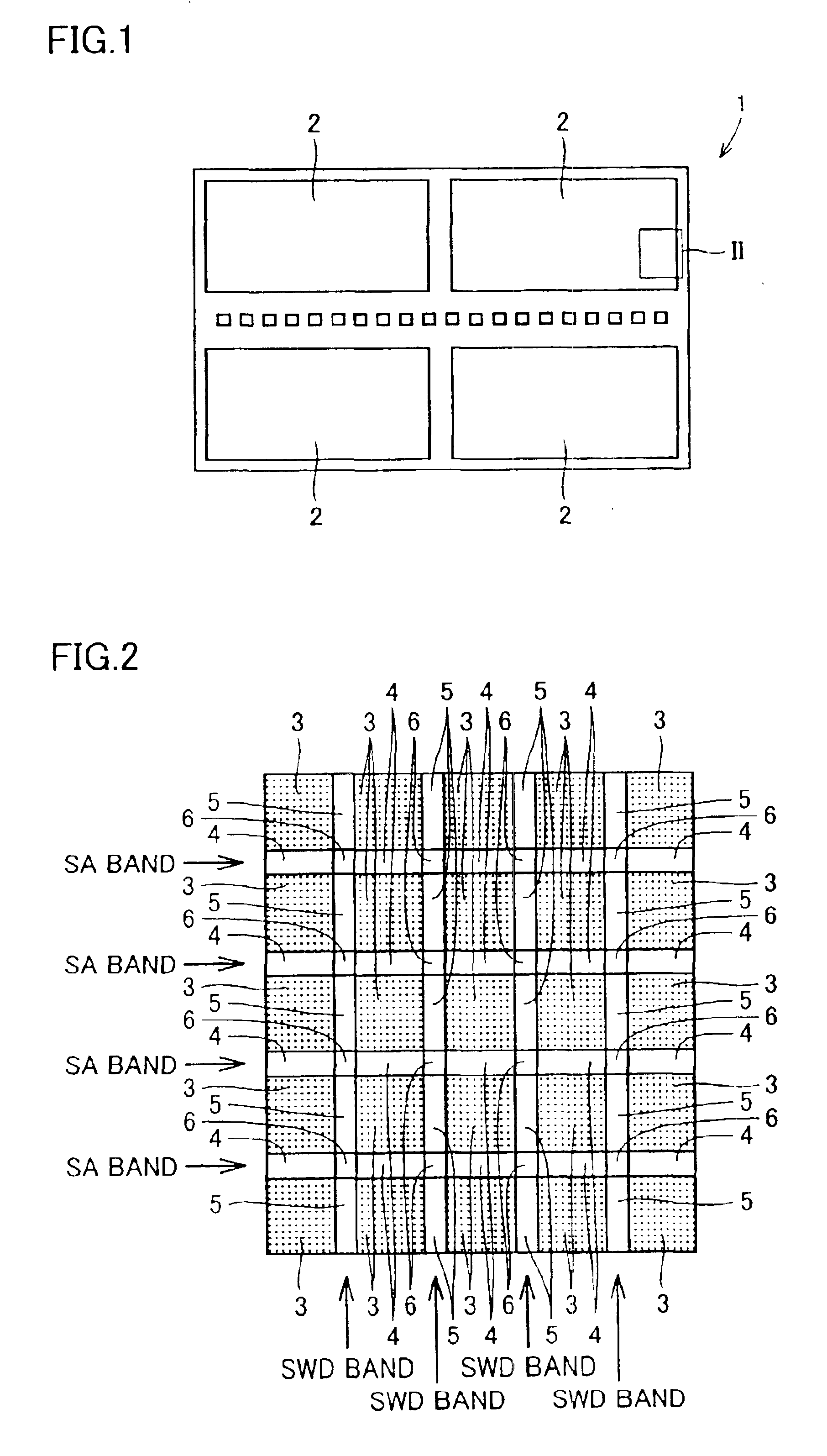
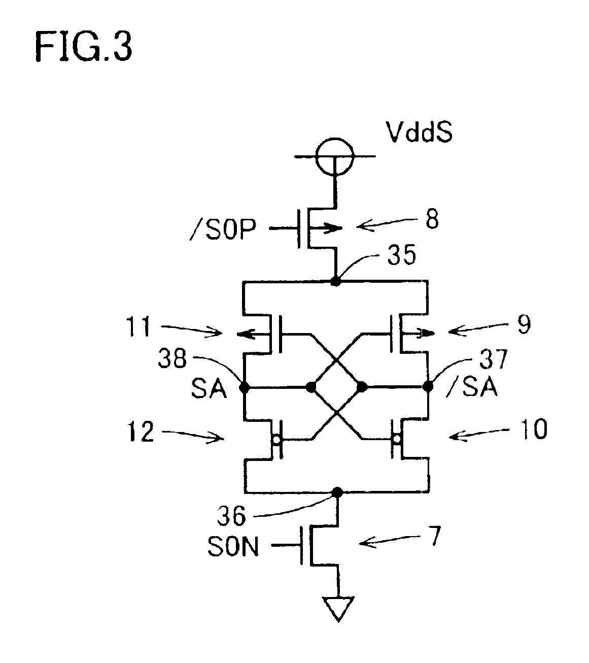
Referring to FIG. 1, the semiconductor memory device in accordance with the present invention is a DRAM in a dispersed word line driving scheme (or a divided word driver scheme), on which chip a plurality of memory cell mats 2 and regions formed with periphery circuits are arranged. Although there are four memory cell mats 2 in a DRAM chip 1 shown in FIG. 1, there may be any number of memory cell mats. Memory cell mat 2 is specifically formed of a plurality of memory cell array regions 3 arranged in a grid (in matrix). Memory cell array regions 3 are separated from each other by a sense ampl...


PUM


Abstract

A semiconductor memory device that can be reduced in chip area while preventing degradation in characteristic is obtained. In DRAM, a plurality of memory cell array regions are arranged in matrix, spaced apart from each other in a row direction and in a column direction, on a semiconductor substrate. A sense amplifier region is arranged in a gap between the memory cell array regions in the column direction. An element forming a sense amplifier is arranged in the sense amplifier region. A subdecoder region is arranged in a gap between the memory cell array regions in the row direction. A cross region is arranged at an intersection of the sense amplifier regions in line and the subdecoder regions in line. A sense amplifier driver element is arranged in the subdecoder region and used in a sense amplifier operation.

Description

BACKGROUND OF THE INVENTION1. Field of the InventionThe present invention relates to a semiconductor memory device, and more particularly to a semiconductor memory device that can be miniaturized and improved in characteristics.2. Description of the Background ArtSemiconductor memory devices such as DRAM (Dynamic Random Access Memory) are conventionally known (see Japanese Patent Laying-Open No. 9-64308, for example).In the semiconductor memory device described in Japanese Patent Laying-Open No. 9-64308, in a memory array configuration in matrix, sense amplifier driving circuits for driving sense amplifiers and I / O control circuits for outputting data from the sense amplifiers are arranged at a plurality of intersection regions of subword drivers dispersedly arranged in a word line direction of the memory array (between memory arrays) and sense amplifiers dispersedly arranged in a data line direction of the memory array (between memory arrays) (intersection regions of strip-like reg...

Claims


Application Information

Patent Timeline
IPC IPC(8): G11C5/02H01L21/8242G11C11/401H01L27/108
CPCG11C5/025
Inventor KAWASAKI, SATOSHI
Owner RENESAS ELECTRONICS CORP
Why Eureka
Try Eureka