Organic electro-luminescence element and the manufacturing method thereof

a technology of electroluminescence element and organic electroluminescence, which is applied in the direction of luminescence screen of discharge tube, transportation and packaging, natural mineral layered products, etc., can solve the problems the decrease of the luminous efficiency, so as to reduce the numerical aperture and the effect of decreasing the numerical aperture of the organic electroluminescence display

Inactive Publication Date: 2005-04-19
BOE TECH GRP CO LTD
View PDF9 Cites 56 Cited by
  • Summary
  • Abstract
  • Description
  • Claims
  • Application Information

AI Technical Summary

Benefits of technology

[0016]However, in the method described in the above publication, because electrode area actually decreases by installing holes in one electrode layer, the numerical aperture of the organic electroluminescence display decreases. Decrease in numerical aperture leads to a decrease in luminous efficiency. Therefore, the method described in the above publication can be enhanced in terms of reducing the consumption of electricity of the organic electroluminescence display.

Problems solved by technology

However, in the method described in the above publication, because electrode area actually decreases by installing holes in one electrode layer, the numerical aperture of the organic electroluminescence display decreases.
Decrease in numerical aperture leads to a decrease in luminous efficiency.

Method used


Image

  • Organic electro-luminescence element and the manufacturing method thereof
  • Organic electro-luminescence element and the manufacturing method thereof
  • Organic electro-luminescence element and the manufacturing method thereof

Examples


first embodiment

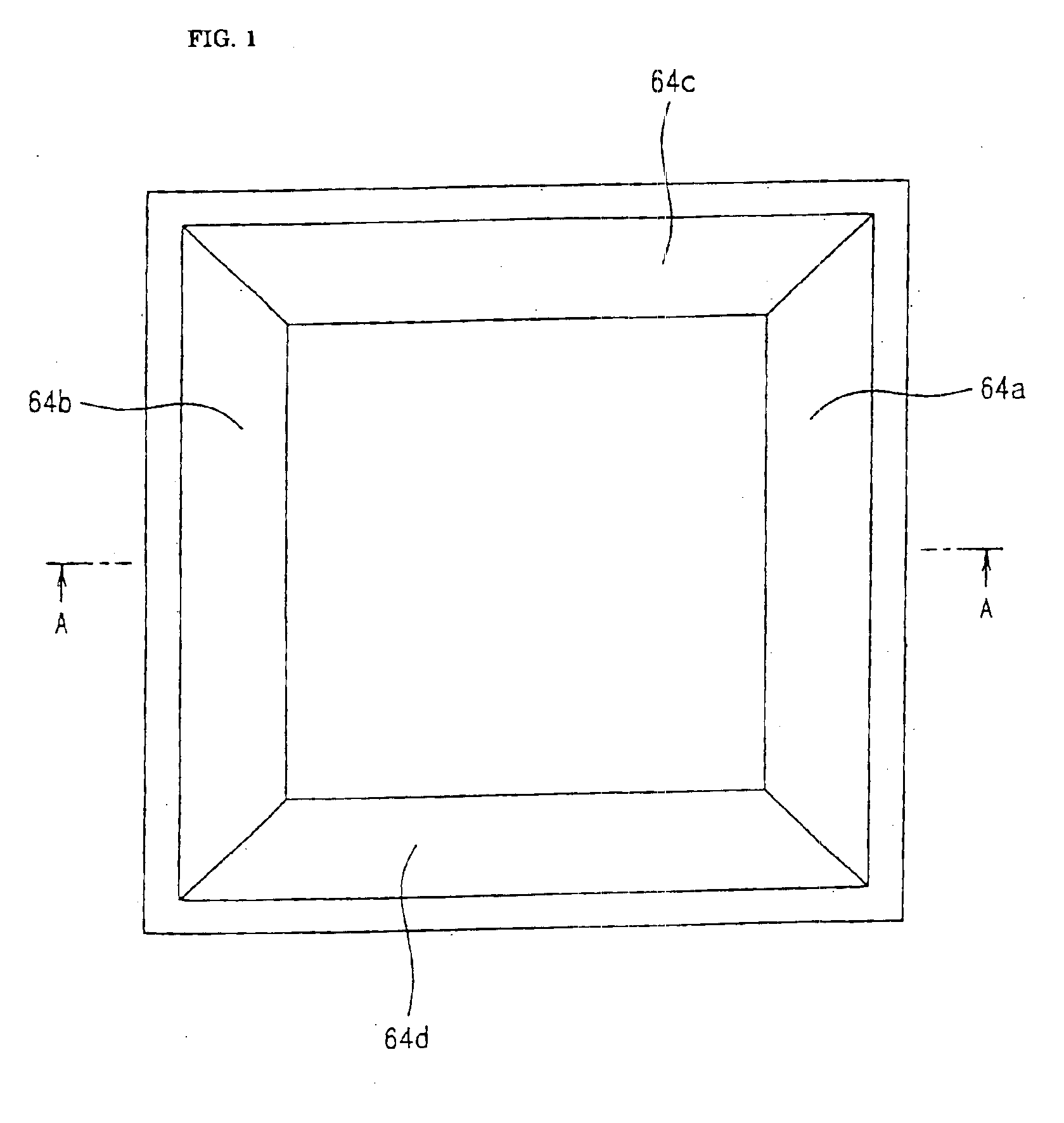
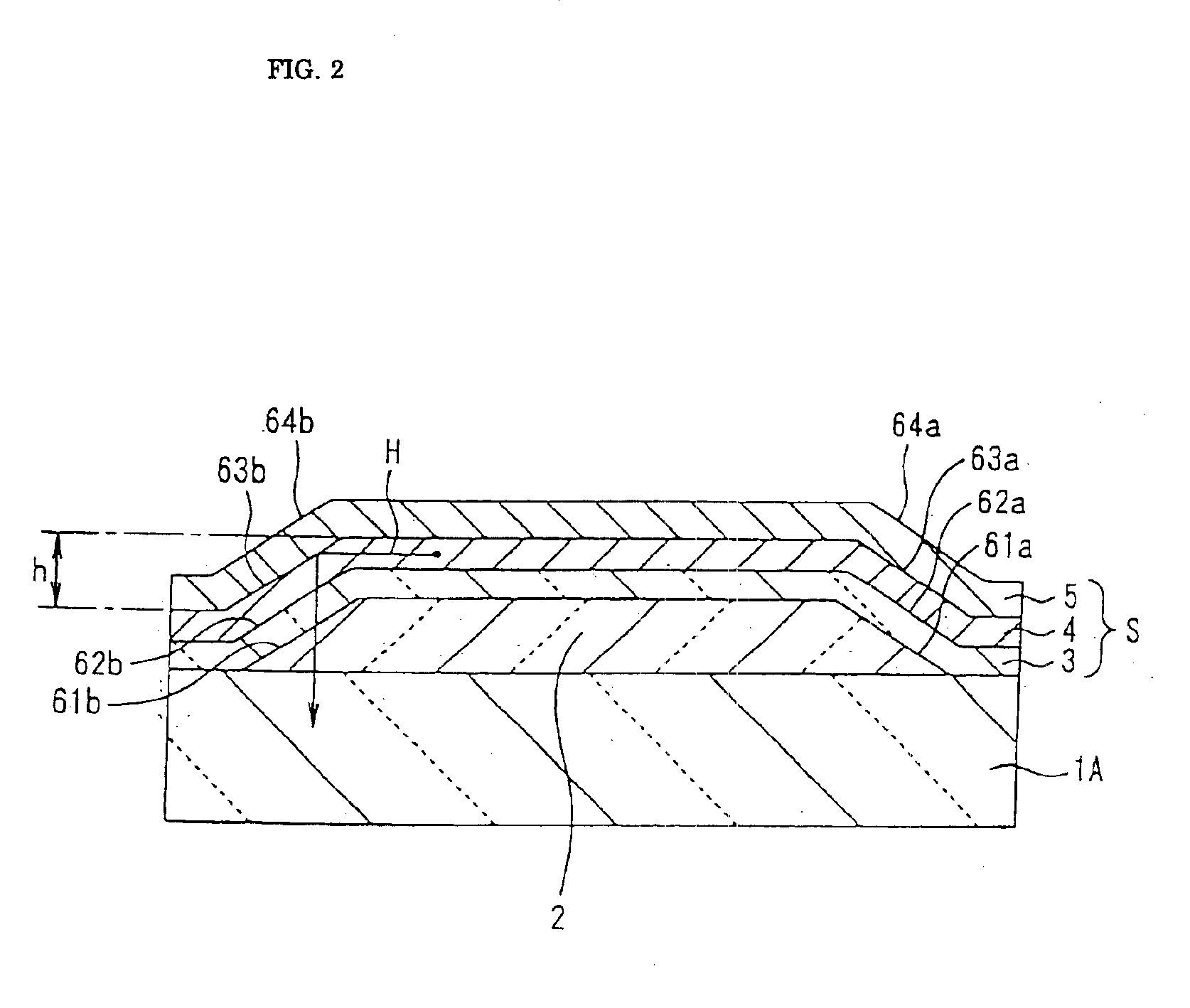
[0058]FIGS. 1 and 2 provide an explanation of an organic electroluminescence display corresponding to the organic electroluminescence element of the present invention. FIG. 1 is a plan view showing an area (an area corresponding to the pixel region divided by the bank 17 in FIG. 11) of the organic electroluminescence display, and FIG. 2 is a sectional view taken along plane A—A of FIG. 1. FIG. 2 shows a glass substrate 1A in the state just before a cumulate body S is formed (a state where many kinds of driving elements are formed on the glass substrate, and the bank 17 is formed).

[0059]On the glass substrate 1A, a cumulate body S is formed via a projection 2 made of a light-transmissive insulating material. This projection 2 is formed by forming a thin film made of light-transmissive materials, such as silicon dioxide (SiO2) and silicon nitride (Si3N4), on the glass substrate 1A, by the plasma CVD method or the sputtering method, at 400 nm in thickness, for example, and then pattern...

second embodiment

[0068]FIGS. 1 and 3 provide an explanation of an organic electroluminescence display corresponding to the organic electroluminescence element of the present invention. FIG. 1 is a plan view showing an area (an area corresponding to the pixel region divided by the bank 17 in FIG. 11) of this organic electroluminescence display, and FIG. 3 is a sectional view taken along plane A—A of FIG. 1. FIG. 3 shows a glass substrate in the state just before a cumulate body S is formed (a state where many kinds of driving elements are formed on the glass substrate, and the bank 17 is formed).

[0069]On this glass substrate 1A, a cumulate body S is formed via a projection 2. The projection 2 is made of an insulating material different from the first insulating film 21 or the first glass substrate 1A. The first insulating film 21 is made of silicon nitride (Si3N4), and the projection 2 is made of silicon dioxide (SiO2).

[0070]The first insulating film 21 is made by the plasma CVD method with a thickne...

third embodiment

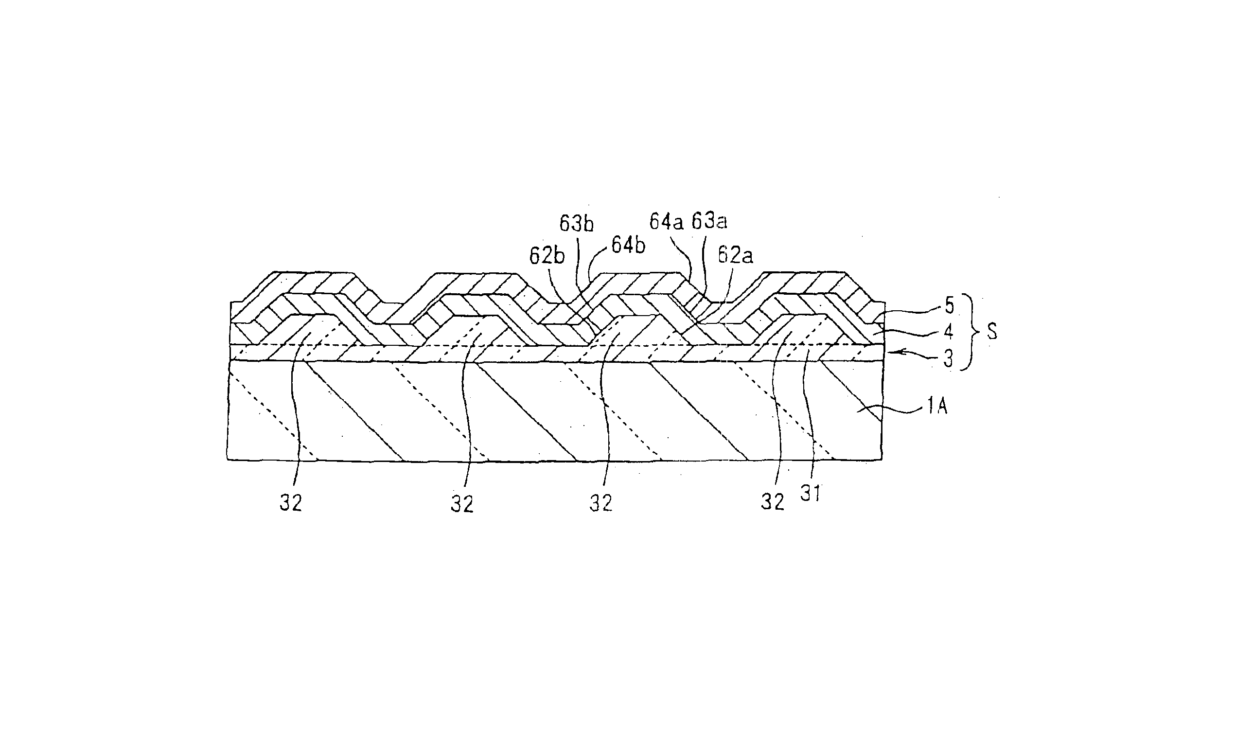
[0079]FIGS. 1 and 4 provide an explanation of an organic electroluminescence display corresponding to the organic electroluminescence element of the present invention. FIG. 1 is a plan view showing an area (an area corresponding to the pixel region divided by the bank 17 in FIG. 11) of this organic electroluminescence display, and FIG. 4 is a sectional view taken along plane A—A of FIG. 1. FIG. 4 shows a glass substrate 1A in the state just before a cumulate body S is formed (a state where many kinds of driving elements are formed on the glass substrate, and the bank 17 is formed).

[0080]In this embodiment, slopes 62-64 of both electrode layers 3 and 5 and an organic luminous layer 4 are formed by making an anode layer (a light-transmissive electrode layer) 3 made of ITO (In2O3—SnO2) in a shape having a convex section 32 corresponding to the slopes. The anode layer 3 is formed in the following method.

[0081]First, the first ITO thin film 31 is made by the sputtering method on the glas...


PUM

PropertyMeasurementUnit
thicknessaaaaaaaaaa
thicknessaaaaaaaaaa
thicknessaaaaaaaaaa

Abstract

The invention increases the outgoing efficiency of light generated in an organic luminous layer of an organic electroluminescence element without decreasing the numerical aperture. A light-transmissive anode electrode layer, an organic luminous layer, and a light-reflective cathode layer are provided on the entire surface of one pixel region. On the anode layer, the organic luminous layer, and the cathode layer, slopes are installed protruding from the anode layer side to the cathode layer side. By this, light generated in the organic luminous layer, and irradiated in parallel to a cumulate surface of a cumulate body, is reflected by the slope on the boundary between the organic luminous layer and the cathode layer and exits toward the anode layer side.

Description

BACKGROUND OF THE INVENTION[0001]1. Field of Invention[0002]The present invention relates to an organic electroluminescence element which is excellent in the output efficiency of light generated in the organic luminous layer.[0003]2. Description of Related Art[0004]Organic electroluminescence displays which are equipped with organic electroluminescence elements (elements having an organic luminous layer between the cathode and the anode) corresponding to the respective pixels have high brightness with spontaneous light. The organic electroluminescence displays can be driven with direct current at low voltage, have a high speed response, and have light generated by a solid organic film. Thus, the organic electroluminescence displays are excellent in display performance and enabling thickness reduction, weight reduction, and electricity consumption reduction. The organic electroluminescence displays are therefore expected to replace liquid crystal displays in the future.[0005]In an or...

Claims


Application Information

Patent Timeline
Patent Type & Authority Patents(United States)
IPC IPC(8): H01L51/52H01L51/50
CPCH01L51/5262Y10T428/2495Y10T428/24479Y10S428/917H10K59/875H10K71/821H10K71/16H10K50/85
Inventor YUDASAKA, ICHIO
Owner BOE TECH GRP CO LTD
Why Eureka
Try Eureka