Self-biasing for common gate amplifier

a gate amplifier and self-biased technology, applied in the direction of pulse technique, pulse manipulation, baseband system details, etc., can solve the problems of affecting the signal transmission over long transmission channels

Inactive Publication Date: 2005-04-19
XILINX INC
View PDF4 Cites 29 Cited by
  • Summary
  • Abstract
  • Description
  • Claims
  • Application Information

AI Technical Summary

Benefits of technology

[0009]Accordingly, the present invention provides a data receiver that compensates for the low pass function of an associated transmission channel. As a result, this data receiver can provide an output data signal that is not prone to inter-symbol interference.
[0011]The exemplary embodiment of the differential amplifier of the present invention advantageously adds a zero to the transfer function of the data receiver, thereby compensating for the pole in the transfer function of the associated transmission channel. That is, the differential amplifier of the present amplifier provides a peaking of the frequency response, which compensates for the low pass transfer function of the associated transmission channel.
[0012]The first and second pads are coupled to source regions of n-channel transistors within the differential amplifier of an embodiment of the present invention. Because the first and second pads are not directly connected to transistor gates within the differential amplifier, the associated ESD protection circuit does not require resistors connected in series with these pads. The absence of such series-connected resistors advantageously eliminates a pole from the transfer function of the data receiver, and enables the data receiver to exhibit a higher frequency transfer function.

Problems solved by technology

At these speeds, signal transmission over long transmission channels are subject to serious problems.
Losses, such as skin effect, dielectric loss, and connector loss become significant at these frequencies.
Higher frequency components of the signal are more adversely affected than lower frequency components due to the low pass nature of the transmission channel.
All wired channel or optical channel applications present a more difficult problem in that the input signal has a large bandwidth.
The low pass transfer function of the transmission channel undesirably attenuates high frequency signals.
Without compensation, this low pass transfer function degrades not only the high frequency amplitudes, but also introduces a form of signal dependent jitter commonly referred to as inter-symbol interference.
However, center region 301 exhibits a relatively small length L1 and width W1, thereby indicating that the transmission of data on the transmission channel is prone to errors due to noise and timing drift.
A small length L1 and width W1 makes signal reception and recovery difficult for the associated data receiver, which usually results in a high bit error rate (BER).
High bit error rate causes packet loss, and thus reduces the effective bandwidth.

Method used


Image

  • Self-biasing for common gate amplifier
  • Self-biasing for common gate amplifier
  • Self-biasing for common gate amplifier

Examples


Embodiment Construction

[0026]In general, the present invention provides a method and apparatus for self-biasing a common gate amplifier, which beneficially provides frequency compensation for high-speed serial input / output (I / O) transmission.

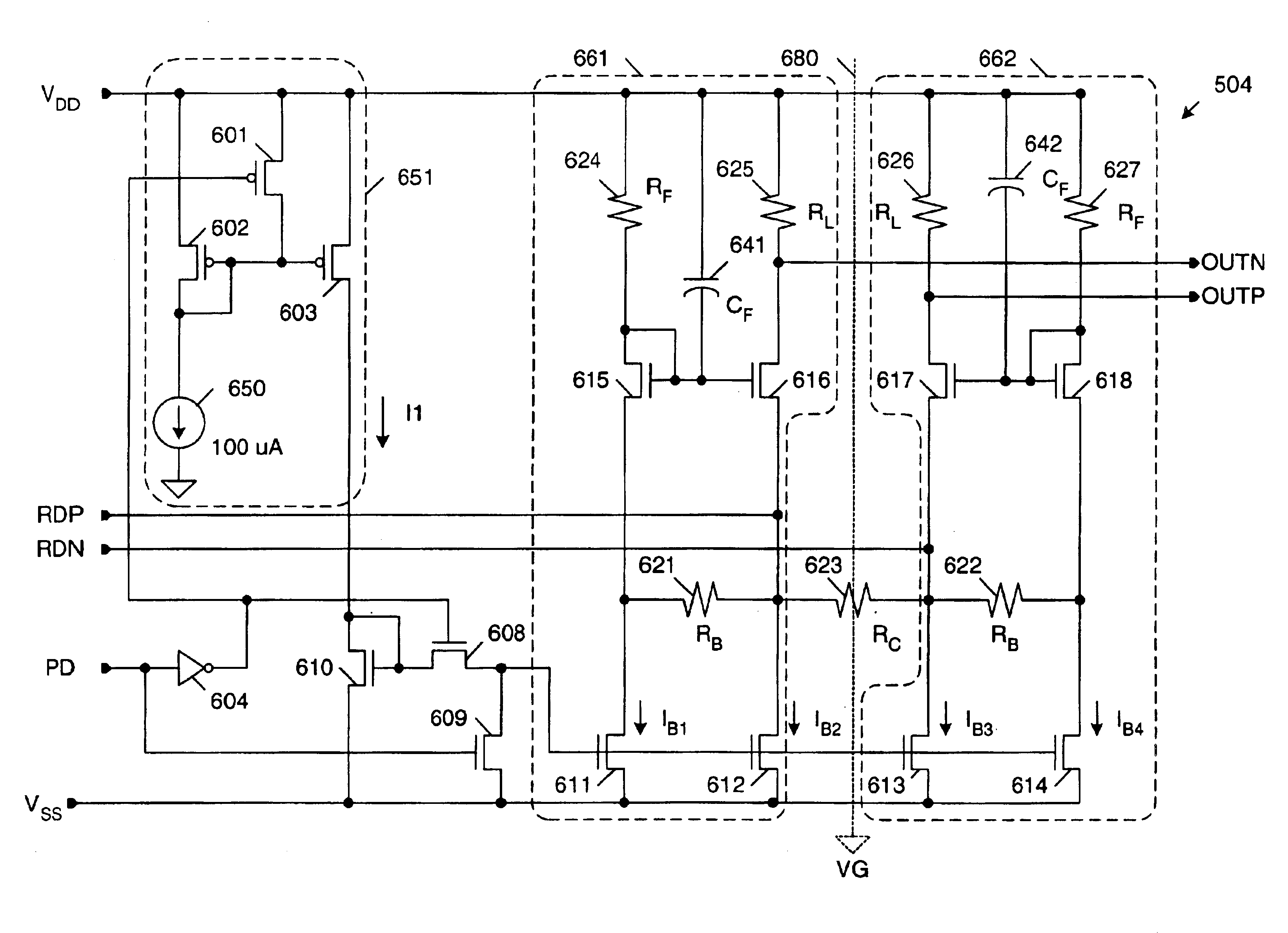
[0027]FIG. 5 is a block diagram of a data receiver 500 in accordance with one embodiment of the present invention. Data receiver 500 includes input pads 501-502, ESD protection circuit 503 and differential amplifier 504. Input pads 501-502 are coupled to receive a differential input signal from transmission channel 510. As described above, transmission channel 510 exhibits a low pass transfer function. Input pads 501-502 are coupled to ESD protection circuit 503, which includes diode elements 511-514. Diode element 511 is coupled between input pad 501 and the VDD voltage supply terminal, and diode element 512 is coupled between input pad 501 and the VSS voltage supply terminal. Similarly, diode element 513 is coupled between input pad 502 and the VDD voltage supply te...


PUM


Abstract

A data receiver having a transfer function that exhibits peaking at high frequencies is provided to compensate an input signal provided on a transmission channel having a low pass transfer function. The data receiver includes first and second differential input terminals, which receive the differential input signal from the transmission channel. The first differential input terminal is coupled to the source of a first common gate transistor in a first self-biased common gate amplifier. The second differential input terminal is coupled to the source of a second common gate transistor in a second self-biased common gate amplifier. A differential output signal is provided from the drain terminals of the first and second common gate transistors. The first and second differential input terminals are not directly connected to any transistor gates in the data receiver, thereby enabling these differential input terminals to be safely connected directly to the transmission channel.

Description

FIELD OF THE INVENTION[0001]The present invention relates to high speed serial I / O on a semiconductor device, and more particularly to a self-biased a common gate amplifier circuit.BACKGROUND OF THE INVENTION[0002]Communications systems are being developed that are capable of handling several hundred or more gigabits per second (GB / s) of bandwidth. At these speeds, signal transmission over long transmission channels are subject to serious problems. Losses, such as skin effect, dielectric loss, and connector loss become significant at these frequencies. Higher frequency components of the signal are more adversely affected than lower frequency components due to the low pass nature of the transmission channel.[0003]All wired channel or optical channel applications present a more difficult problem in that the input signal has a large bandwidth. With a large bandwidth signal, there are varying degrees of signal degradation that are signal dependent. FIG. 1 is a graph illustrating a typic...

Claims


Application Information

Patent Timeline
Patent Type & Authority Patents(United States)
IPC IPC(8): H03F1/30H03K5/02H04L25/02H04L25/03
CPCH03F1/301H03F3/45179H04L25/0292H04L25/03878H03K5/023H03F2200/444H03F2200/72
Inventor GABOURY, MICHAEL J.GROEN, ERIC D.
Owner XILINX INC
Why Eureka
Try Eureka