Method for error reduction in lithography

Inactive Publication Date: 2005-04-19
MICRONIC LASER SYST AB
View PDF15 Cites 125 Cited by
  • Summary
  • Abstract
  • Description
  • Claims
  • Application Information

AI Technical Summary

Problems solved by technology

Of course the predictions are less certain the farther into the future we look and nobody knows if the electronics industry will still be using transistors in the year 2020.
Either way it will be difficult to achieve the needed pattern fidelity.
Furthermore, it can also be distorted by the built-in stress in surface films deposited on it and by the patterning of said films.
Clamping deformation gives a placement or registration error.
Another large source of placement errors in the finished product is the distorsion in the exposure tool, be it a wafer stepper for semiconductors or a projection aligner for display panels.
The placement can also be affected by processing, both because films deposited on or removed from a workpiece have built-in stress and deform the workpiece, and because some process steps cause a shrinkage or warping of the workpiece, e.g. high temperature annealing steps.
An important s

Method used


Image

  • Method for error reduction in lithography
  • Method for error reduction in lithography
  • Method for error reduction in lithography

Examples


Embodiment Construction

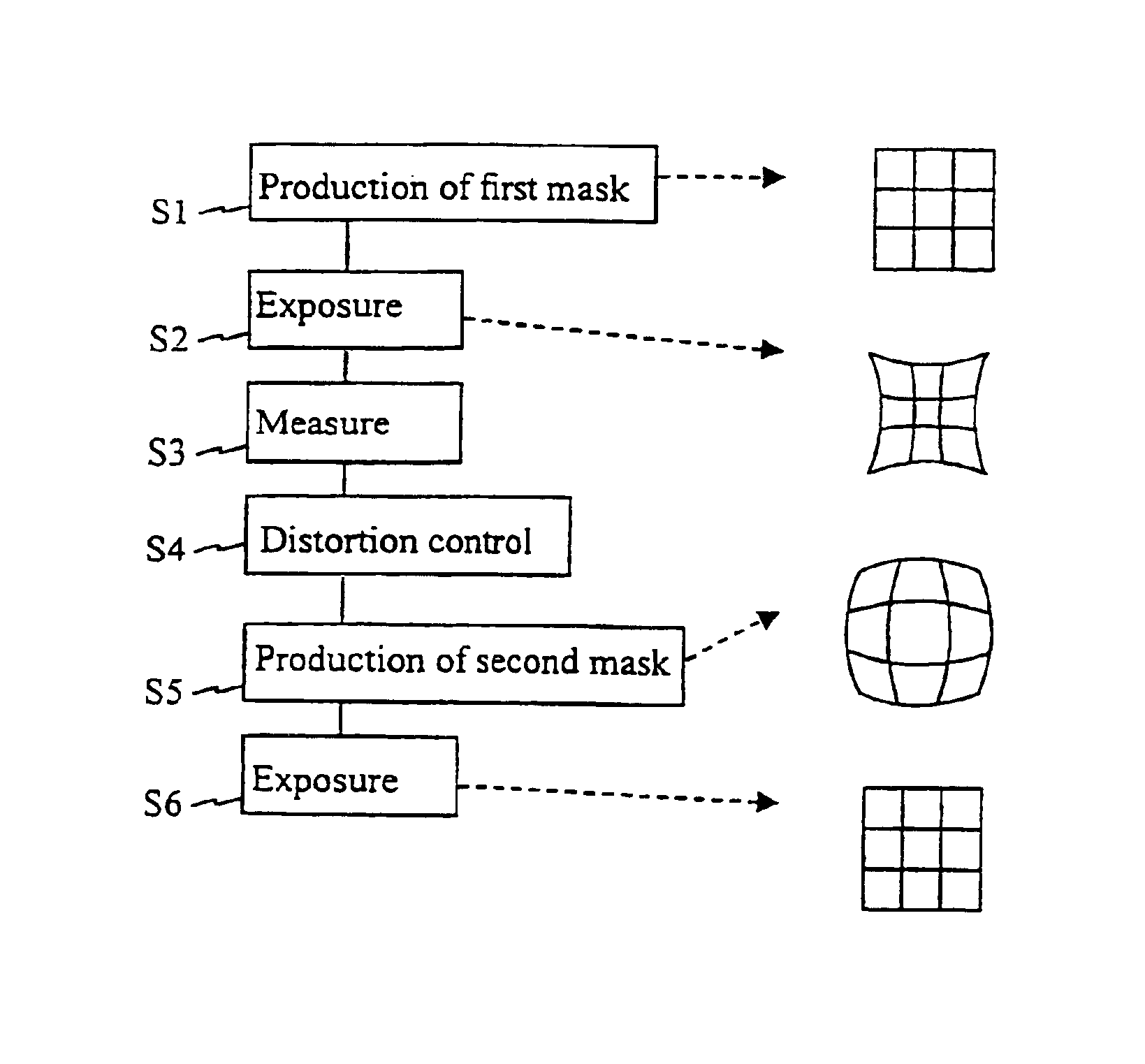
[0032]The invention is best described as a control system, such as is shown in FIG. 5. The pattern picks up errors 501, 502 of different kinds when it is converted from a design data file 503 and a mask blank 504 to a mask 505 during a mask writing procedure 506, i.e. exposure, by means of a mask writer 507. The mask is thereafter used to produce an electronic device 508. The pattern file describes what the chip or panel designer wants to see printed and any deviation is to him an error. One part of these errors is that systematic and other errors are different from one time to another. The invention is based on the identification of different types of errors and the appropriate way to reduce each type. Errors that can be found in the output from the system and identified to be recurring in a systematic fashion are reduced by feeding an inverse error 509 back to the writing of the mask. This is the feed-back loot 510 in FIG. 5. The feed-back can be pseudo-continuous, i.e. correction...


PUM


Abstract

The present invention relates to a method and a system for predicting and correcting geometrical errors in lithography using masks, such as large-area photomasks or reticles, and exposure stations, such as wafer steppers or projection aligners, printing the pattern of said masks on a workpiece, such as a display panel or a semi-conductor wafer. The method according to the invention comprises the steps of collecting information about a mask substrate, a mask writer, an exposure stati n, and/or about behavior of a processing step that will occur after the writing of the mask. Further the method comprises predicting from the combined information distorsions occuring in the pattern, when it is subsequently printed on the workpiece; calculating from said prediction a correction to diminish said predicted distorsion, and exposing said pattern onto said mask substrate while applying said correction for said distorsions.

Description

[0001]This application is the national phase under 35 U.S.C. § 371 of PCT International Application No. PCT / SE00 / 01030 which has an International filing date of May 22, 2000, which designated the United States of America and was published in English.FIELD OF THE INVENTION[0002]The invention relates to production and precision patterning of photomasks and use of such photomasks in microlithography, for example in the production of flat panel displays and semiconductor circuits. Errors in the pattern on the display panel or semiconductor chip can be separated into errors from systematic sources, from the interaction of maskblank and pattern with the equipment, and from random fluctuations. The invention relates to the reduction of these errors. In a different sense the invention relates to the characterization of the photomask substrate and the equipment and processes used with a photomask, the storage and retrieval of information obtained by such characterization, and the generation ...

Claims


Application Information

Patent Timeline
IPC IPC(8): G03F1/00G03F7/20G03F1/14H01L21/027
CPCG03F7/704G03F7/70433G03F7/70783G03F7/706G03F7/70616G03F7/705G03F1/144G03F1/72
Inventor SANDSTROM, TORBJORNEKBERG, PETERASKEBJER, PEREKBERG, MATSTHUREN, ANDERS
Owner MICRONIC LASER SYST AB
Why Eureka
Try Eureka