Wafer container

a container and wafer technology, applied in the field of wafer containers, can solve the problems of increasing costs, reducing device yield, and difficult to furthermore purify the clean room environment itself, so as to reduce production costs, improve production efficiency, and shorten the cycle time of production.

Inactive Publication Date: 2005-04-26
KK TOSHIBA
View PDF18 Cites 43 Cited by
  • Summary
  • Abstract
  • Description
  • Claims
  • Application Information

AI Technical Summary

Benefits of technology

[0013]The present invention has been made in order to solve the shortcomings as described above. It is an object of the present invention therefore to provide a container for storing substrates capable of shortening the cycle time of the production, improving the production efficiency and reducing the production cost is provided.

Problems solved by technology

The major causes of lessening the device yield is the existence of contaminant particles consisting of dust, organic substances and so forth.
However, the size of the contaminant particles to be eliminated has been decreased along with the miniaturization of LSIs and the rapidly increasing packing densities and therefore it is difficult to furthermore purify the clean room environment itself in view of avoiding an increase in costs.
Particularly, substantial adverse effects are likely in the case of highly miniaturized LSIs.
Namely, the transportation of the wafer pod is delayed by the gas filling time.
Accordingly, there is a problem that the cycle time required for completing all the manufacturing steps is elongated by the gas filling time resulting in deteriorating the effectiveness of the manufacture process, and then an increase in costs.
On the other hand, the semiconductor process chamber of the subject manufacturing step is left idling during the period that the previous wafer pod is being filled with the gas so that the process chamber is used in an ineffective manner.
The accumulated loss time is considered to be substantial.
Accordingly, in the same manner as the above (1), it results in elongating the cycle time required for completing all the manufacture process and deteriorating the effectiveness of the manufacture process, and then an increase in costs.

Method used


Image

  • Wafer container
  • Wafer container
  • Wafer container

Examples


first embodiment

[0038](First Embodiment)

[0039]As illustrated in FIG. 2, a semiconductor wafer transportation pod in accordance with the present invention is placed on a wafer pod table 20 located in front of a semiconductor process chamber 26 when semiconductor wafers 10 are carried out from the semiconductor process chamber 26 or are carried in the semiconductor process chamber 26. In usual cases, 2 to 4 wafer pod tables 20 are assigned to one semiconductor process chamber 26. The wafer pod table 20 is used to support the semiconductor wafer transportation pod that is transported from the previous semiconductor process chamber 26 for use in the previous manufacturing step. The pod lid 14 is detached from the wafer pod body 12 after placing the wafer pod. The detachment of the pod lid 14 is performed by means of the lid opening / closing control means 22. The lid opening / closing control means 22 is also used to fix the pod lid 14 to the wafer pod body 12. In another case, these procedures may be manu...

second embodiment

[0064](Second Embodiment)

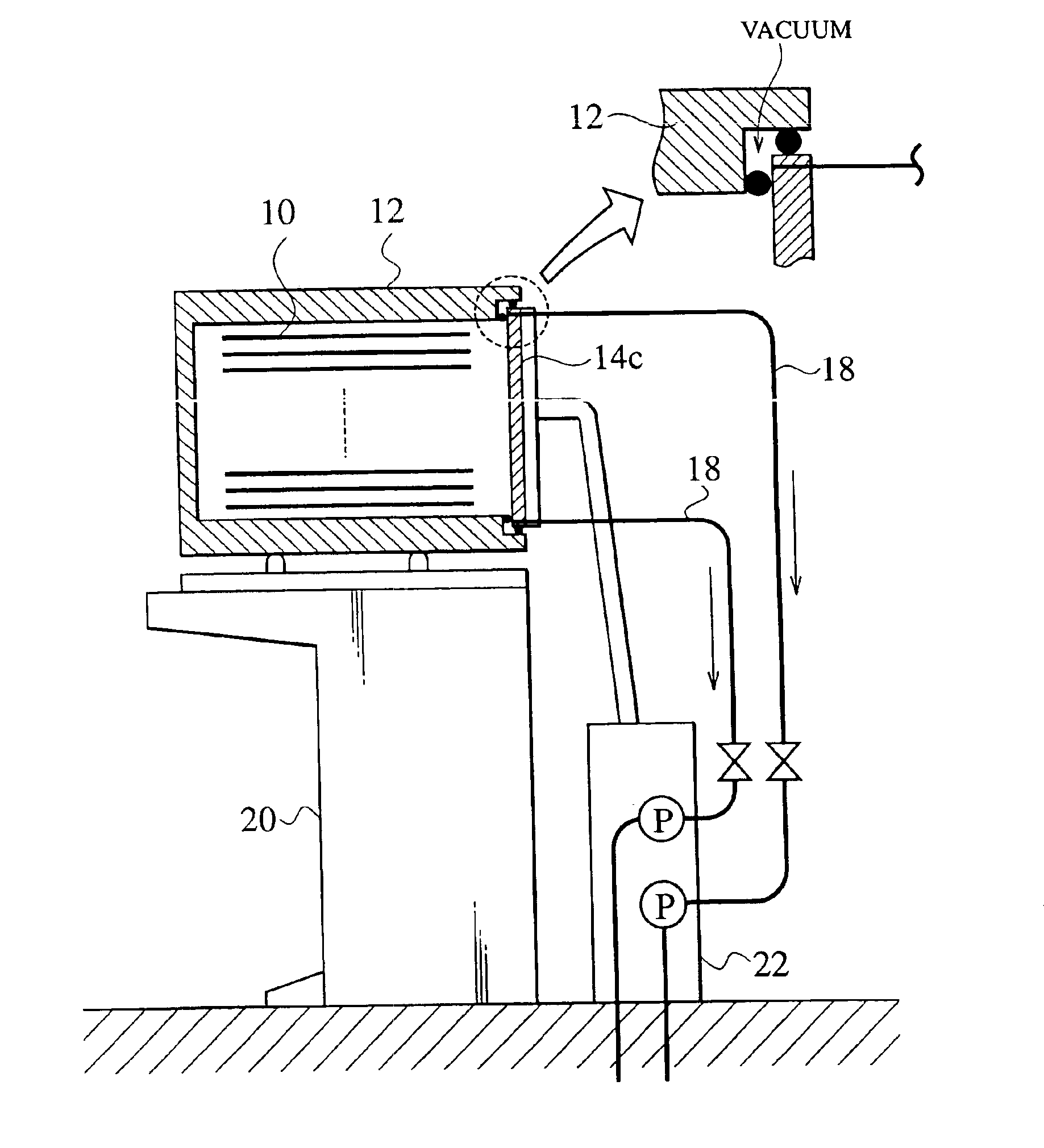
[0065]Next, the second embodiment of the present invention will be explained. The second embodiment of the present invention is described to show an example which is capable of improving the sealing ability of the wafer pod and also improving the leak-proof structure of the wafer pod by evacuating the interior of the wafer pod into a vacuum condition.

[0066]FIG. 9A is a schematic diagram showing the wafer transportation by means of a semiconductor wafer transportation pod in accordance with the second embodiment of the present invention which is placed on a wafer pod table 20 for carrying in or out the semiconductor wafers 10. FIG. 9B is a schematic diagram showing the semiconductor wafer transportation pod in accordance with the second embodiment of the present invention which is transported between the process chambers. As illustrated in FIG. 9A, in the case of the semiconductor wafer transportation pod according to the second embodiment of the present inve...


PUM

PropertyMeasurementUnit
diameteraaaaaaaaaa
pressureaaaaaaaaaa
mechanicalaaaaaaaaaa

Abstract

A container for storing substrates capable of shortening the cycle time of the production, improving the production efficiency and reducing the production cost is provided. The container for storing substrates is composed of a box for accommodating the substrates, and a closure member for sealingly closing the box by tightly fixing the closure member to the opening of the box. The container for storing substrates is provided with means for temporarily storing a sealing gas and introducing the sealing gas into the box. Also, the container for storing substrates is provided with means for means for temporarily forming a low pressure space for the purpose of evacuating the gas inside of the box by transferring the gas to the low pressure space.

Description

CROSS REFERENCE TO THE RELATED APPLICATION[0001]This application is a continuation of U.S. Ser. No. 09 / 605,894 filed Jun. 29, 2000, abandoned,[0002]The subject application is related to subject matter disclosed in the Japanese Patent Application No. Hei11-186768 filed in Jun. 30, 1999 in Japan, to which the subject application claims priority under the Paris Convention and which is incorporated by reference herein.BACKGROUND OF THE INVENTION[0003]1. Field of the Invention[0004]The present invention is related generally to a transportable container for storing substrates such as a semiconductor wafer transportation pod for accommodating a stack of semiconductor wafers. In particular, the present invention is related to a SMIF (Standard Mechanical Interface)-type semiconductor wafer transportation system for accommodating a stack of semiconductor wafers in a SMIF-type box and transporting the stack of semiconductor wafers between the process chambers.[0005]2. Description of the Relate...

Claims


Application Information

Patent Timeline
Patent Type & Authority Patents(United States)
IPC IPC(8): H01L21/677H01L21/67H01L21/673H01L21/68
CPCH01L21/67376H01L21/67772Y10T137/86083
Inventor INOUE, KIYOTAKAMUGURUMA, TERUMIKURODA, YUICHIYOSHIKAWA, NORIAKI
Owner KK TOSHIBA
Why Eureka
Try Eureka